
Electronics product design is the process of taking a product concept through circuit design, PCB layout, firmware development, design for manufacture and compliance to arrive at a production-ready hardware product. This guide is written for hardware startup founders, product owners and engineering managers who want a clear-eyed view of what the design process actually involves, where costs accumulate, and what risks most commonly derail first-time hardware products. Whether you are evaluating a design partner or trying to understand what you are buying, this guide maps the full picture.
TL;DR
- Electronics product design spans feasibility, schematic capture, PCB layout, firmware, prototyping, DFM, compliance and production handover.
- Most cost overruns trace back to three causes: unclear requirements, late DFM, and compliance discovered at the end of the project rather than the beginning.
- Component selection in 2026 requires active obsolescence and supply risk management – structural cost pressures mean reactive BOM decisions are expensive.
- A staged design process with defined deliverables at each gate reduces risk more than trying to compress all phases into a single sprint.
- Fixing a design error during prototype costs roughly 10x more than catching it during schematic review, and 100x less than a field recall.
- Zeus Design offers end-to-end electronics design, rapid prototyping and DFM services for Australian hardware product teams.
Why Electronics Product Design Is Harder Than It Looks
Most hardware founders underestimate the number of disciplines that need to work together before a product is ready for manufacture. Electronics product design is not just circuit design. A completed, manufacturable hardware product requires aligned decisions across analog and digital circuit architecture, PCB layout and signal integrity, firmware and hardware integration, mechanical-electrical interface, thermal management, component availability, compliance with regulatory standards, and production yield engineering.
Miss any one of these and you do not just face a delay – you face a redesign. According to DE Design Works, unclear or incomplete product requirements are the single leading cause of cost overruns and schedule failures in new electronic product development. The second most common cause is discovering compliance requirements late, which can add months and significant cost to a product launch.
This guide walks through the full workflow, the risks at each stage, and the cost dynamics that product teams most commonly underestimate.
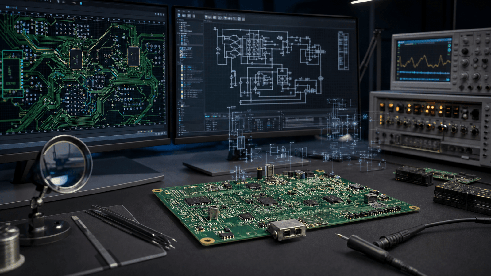
What Electronics Product Design Includes
A full-scope electronics product design engagement typically covers the following phases. Not every project needs all of them in sequence, but all of them need to be considered and deliberately scoped in or out.
1. Feasibility and Requirements Definition
Before any circuit is drawn, a well-run project starts with a requirements definition phase. This establishes what the product must do, the electrical and physical constraints, the target operating environment, the intended regulatory markets, and a preliminary bill of materials (BOM) cost target. Projects that skip this phase almost always revisit it later – after redesign costs have accumulated.
Feasibility analysis is also where major architecture decisions are made: processor selection, wireless connectivity approach, power architecture, and sensor selection. These upstream decisions have cascading effects on PCB layout, firmware complexity, and certification pathway. Changing them mid-project is expensive.
2. Circuit Design and Schematic Capture
The schematic is the foundation document for the entire design. Circuit design covers both analog and digital subsystems, power supply design, protection circuitry, and signal conditioning. A well-constructed schematic is also the primary tool for catching design errors before they are committed to a physical board.
Good schematic practice includes component selection rationale, design margins for temperature and tolerance, and explicit decisions about EMC – which filtering components are placed where, and why. Schematic reviews at this stage are significantly cheaper than discovering the same issues during prototype testing or compliance testing.
3. PCB Layout and Signal Integrity
PCB layout translates the schematic into a physical board design. For simple products this is straightforward. For products with high-speed digital interfaces, RF sections, precision analog measurement, or high-current power paths, PCB layout is a significant engineering exercise in its own right.
Signal integrity, EMC management, impedance control, thermal management and design for manufacture (DFM) are all primarily resolved at the layout stage. A layout that ignores EMC or thermal concerns will produce a prototype that fails compliance testing or runs too hot in the field. Patton Electronics notes that DFM issues not caught at the layout stage are among the most costly to address once boards are in fabrication.
4. Prototyping and Bring-Up
The first physical prototype is where the design assumptions are tested against reality. Prototype bring-up involves board power sequencing, peripheral initialisation, firmware loading, and systematic functional testing. Issues found at this stage – wrong footprints, marginal power rails, grounding problems, software-hardware timing conflicts – are resolved here before the design is locked.
Most hardware products require two to three prototype iterations before reaching a design that is ready for DFM review. Planning for this is not pessimism – it is standard engineering practice. A single-prototype-to-production schedule is realistic only for very simple boards with highly experienced teams.
5. Firmware and Hardware Integration
Electronics product design is not complete without working firmware. Firmware and hardware need to be developed in parallel, not sequentially. When firmware development is deferred until after hardware is finalised, teams consistently discover hardware issues that require board respins – peripheral register maps that do not match the selected microcontroller, I/O voltage levels that are incompatible, timing requirements that cannot be met in software.
Developing firmware alongside hardware – and bringing up each subsystem as hardware becomes available – catches these issues at the lowest possible cost and keeps the overall schedule on track.
6. Design for Manufacture (DFM)
DFM is the process of reviewing and adapting the design to ensure it can be assembled reliably and cost-effectively at production volumes. DFM covers PCB panelisation and fiducial placement, component clearances for automated pick-and-place, solder paste apertures, via-in-pad restrictions, component orientation for efficient assembly flow, and test access point placement.
According to Fenix Manufacturing’s 2026 DFM analysis, DFM reviews integrated early in the design process – rather than applied as a final check – have the largest impact on production yield and unit cost. Early DFM also avoids the scenario where a design is already prototyped and verified functionally, but requires significant rework to be manufacturable.
7. Compliance and Certification Planning
Most electronic products sold in Australia, the US or Europe require some form of regulatory certification. Common certifications include ACMA compliance (RCM mark) for Australian radio and electrical products, CE marking for Europe, and FCC for the US. Products with wireless modules also need to comply with the wireless module manufacturer’s integration requirements to maintain module certification.
Compliance is not a final step – it is a design input. Products designed with compliance requirements in mind from the schematic stage have significantly lower certification risk and fewer pre-compliance test failures. Products where compliance is an afterthought frequently require board respins after EMC pre-compliance testing.
When a Project Needs Professional Electronics Design
Hardware founders sometimes try to reduce upfront cost by fragmenting the design process – using freelancers for schematic capture, a separate contractor for PCB layout, and another person for firmware. This approach can work for very simple products, but it consistently creates integration risk on anything with real complexity. The interfaces between disciplines – schematic-to-layout, layout-to-firmware, firmware-to-cloud – are where the costly problems accumulate when there is no continuity of design ownership.
A professional electronics product design engagement makes most sense when:
- The product has multiple subsystems that need to work together reliably (power, sensing, wireless, display, cloud connectivity).
- The product needs to pass regulatory certification in one or more markets.
- The team is targeting a defined production volume where BOM cost and yield matter.
- There is a real timeline – missed windows have commercial consequences.
- The team does not have in-house electronics engineering resources with the required depth.
For simpler products – a single-function board with a known microcontroller and no wireless – a well-briefed freelancer may be entirely adequate. Knowing the difference before you start saves time and cost.
Technical and Commercial Risks to Manage
The risks in electronics product design cluster into four main categories. Understanding them before the project starts lets you scope your design engagement to manage them explicitly rather than discovering them mid-project.
Requirements Drift
Scope changes during the design phase are the most common driver of budget and schedule overruns. Adding a wireless interface, changing the target microcontroller, adding a new sensor, or revising the mechanical envelope mid-layout each trigger cascading changes through schematic, layout and firmware. The best mitigation is thorough requirements definition before design starts, with a formal change control process for anything that comes later.
Component Availability and Cost
In 2026, component supply and cost management is a significant design input, not just a procurement concern. According to Accuris, 72% of electronics product teams report $50,000 or more annually in costs from reactive component decisions, and 68% make six or more component changes per project. Structural cost pressures from raw material prices, memory chip demand, and supply chain disruption mean that component selection decisions made during schematic design need to explicitly consider second-source availability and lifecycle status.
Discovering component obsolescence after a product is in production can force an emergency redespin costing $50,000-$500,000 and taking 6-12 months. Proactive obsolescence planning during design is materially cheaper.
Compliance and Certification Risk
Certification timelines are fixed minimums – no amount of urgency or budget can compress a regulatory test window. A product that fails EMC pre-compliance testing one month before a planned product launch faces a realistic delay of three to six months while design changes are made, boards are re-fabricated, and testing is repeated. The cost is the test fees plus the redesign plus the missed launch window.
Compliance-aware design from the start – appropriate filtering, controlled impedances, proper grounding, certified wireless modules integrated correctly – materially reduces this risk.
Firmware-Hardware Integration Failures
Late firmware integration is one of the most common causes of unexpected board respins. A hardware design that looks complete on paper can still require a new PCB revision when firmware bring-up reveals that a pin assignment conflicts with a peripheral’s required function, or that a communication bus does not meet the timing requirements of a sensor. Parallel hardware and firmware development, with progressive bring-up against the actual PCB, is the standard risk-reduction approach.
Cost Structure: Where the Money Goes
Electronics product design costs vary significantly by project complexity, but the cost structure is broadly consistent. Understanding where costs accumulate helps product teams scope engagements and avoid the most expensive surprises.
| Phase | Typical cost drivers | Cost of getting it wrong |
|---|---|---|
| Requirements and feasibility | Engineering time, architecture decisions | Redesign through all subsequent phases |
| Circuit and schematic design | Engineering time, component selection research | PCB respin plus firmware rework |
| PCB layout | Layout engineer time, CAD tooling | Prototype failure, compliance failure, DFM rework |
| Prototyping and bring-up | Board fabrication, assembly, components, test time | Second or third prototype iteration |
| Firmware development | Software engineering time, hardware integration | Late-stage board respin, schedule overrun |
| DFM review | DFM engineer time, potential layout revision | Poor production yield, assembly cost blowout |
| Compliance and certification | Test house fees, pre-compliance testing, retesting | Missed launch window, redesign and retest cycle |
The rule of thumb cited in engineering practice is that fixing a design error costs roughly 10x more at each successive stage: $10 at schematic review, $100 at PCB prototype, $1,000 during production, $10,000 or more as a field failure. Front-loading design rigour and review time is not caution for its own sake – it is cost management.
For a detailed look at project cost structures, ByteSnap’s electronic product design cost guide covers typical cost ranges by project complexity and region.
Zeus Design’s Electronics Product Design Process
Zeus Design’s electronics design service covers the full workflow from concept to production-ready hardware. Engagements are structured around defined design phases with review gates, so clients have visibility into progress and can validate direction before the next phase begins.
The process covers:
- Concept and requirements workshop – establishing functional requirements, constraints, target markets and compliance pathway before any design work begins.
- Circuit architecture and schematic design – including component selection with supply risk and cost considerations factored in from the start.
- PCB layout using Altium Designer, with EMC-aware routing, signal integrity management and DFM incorporated during layout rather than applied as a post-review.
- Rapid prototyping via Zeus Design’s rapid prototyping service, with quick-turn board fabrication and functional bring-up to validate the design at each iteration.
- Firmware development in parallel with hardware, with progressive integration and testing against the actual PCB.
- DFM review and production handover – reviewing the design against the intended manufacturing process, optimising for yield and assembly cost, and preparing the full production package for the contract manufacturer.
Where products require IoT connectivity, cloud backends, or mobile app integration, Zeus Design’s electronics design team works alongside the software development team to ensure hardware-software interfaces are resolved during design – not discovered during integration.
For teams earlier in the process who want to validate a concept before committing to full electronics design, Zeus Design’s rapid prototyping service includes proof-of-concept builds using development modules and off-the-shelf components to test core functionality before custom electronics are designed.
How Electronics Design Connects to Related Services
Electronics product design rarely exists in isolation. For most connected hardware products, the electronics design phase is one part of a broader development effort that also includes firmware, a mobile app, and a cloud backend. The integration points between these workstreams are where problems cluster when different providers are managing each piece independently.
Zeus Design’s electronics design work is connected directly to:
- Circuit board design and PCB layout – handled in-house using Altium, with schematic-to-layout continuity and DFM built into the process.
- Embedded software development – firmware developed alongside hardware to avoid late-stage interface failures.
- IoT connectivity design – wireless protocol selection, antenna integration and cloud-ready architecture built into the hardware design from the start.
- Test jig development – custom test fixtures for production validation, developed from knowledge of the product’s circuit architecture.
For more on the stages of an electronics development engagement, see Zeus Design’s guide to electronics design from concept to production and the breakdown of electronics development stages, risks and costs.
FAQs
What does electronics product design actually involve?
Electronics product design covers the full process of taking a product concept to a production-ready hardware design. That includes requirements definition, circuit and schematic design, PCB layout, firmware development, prototyping and bring-up, design for manufacture, and compliance planning. The scope varies by product complexity, but all of these phases need to be accounted for in any realistic project plan.
How long does an electronics product design project take?
A simple single-board product with no wireless and a known microcontroller platform can be taken from schematic to functional prototype in 8-12 weeks. A connected product with wireless, cloud integration, firmware and compliance requirements typically takes 6-12 months from requirements to production-ready design, including two or three prototype iterations. Timelines lengthen most reliably when requirements change mid-project or when compliance is addressed late.
What are the biggest risks in electronics product design?
The four most common risk categories are: unclear requirements leading to scope changes mid-design; compliance requirements discovered late in the project; component obsolescence or supply disruption affecting the BOM; and late firmware-hardware integration revealing design issues that require a board respin. Each is manageable with front-loaded planning – and each is significantly more expensive to address once the design is in prototype or production.
How much does electronics product design cost in Australia?
Cost varies substantially by product complexity, number of prototype iterations, and service scope. A straightforward single-board product might cost $15,000-$40,000 AUD for design and first prototype. A multi-board connected product with firmware, DFM and compliance support could range from $80,000-$200,000 AUD or more. The most reliable way to scope costs is to engage a design partner for a requirements definition phase before committing to a full design budget. See also ByteSnap’s electronic product design cost reference for international benchmarks.
What is DFM and why does it matter for hardware startups?
Design for manufacture (DFM) is the process of reviewing and adapting a PCB design to ensure it can be assembled reliably and cost-effectively at production volumes. For hardware startups, DFM is particularly important because prototype-quality assembly tolerances do not reflect production reality. A design that works at five units can fail at yield when scaled to 500. DFM reviews conducted during layout – rather than as a final gate check – have the greatest impact on production cost and assembly quality. See Zeus Design’s electronics design service for how DFM is integrated into the design process.
When should a startup use a design house versus a freelancer for electronics product design?
Freelancers can be cost-effective for well-scoped, lower-complexity electronics work where the product team has the expertise to manage integration across disciplines. A design house makes more sense when the product has multiple interacting subsystems, requires compliance certification, has a real commercial timeline, or needs firmware developed alongside hardware. The risk of fragmented responsibility across freelancers grows proportionally with product complexity and integration depth.
How does Zeus Design approach electronics product design for startups?
Zeus Design structures engagements around defined phases with review gates – concept and requirements, circuit design, PCB layout, prototyping, firmware, DFM and production handover. For startups, this phased approach provides cost visibility and decision points before committing to the next phase. Zeus Design’s electronics, firmware and software teams work together on connected products, which reduces integration risk at hardware-software boundaries. More information is available at the Zeus Design electronics design service page.
Conclusion
Electronics product design is a multi-discipline engineering process that spans circuit architecture, PCB layout, firmware, prototyping, DFM and compliance. For hardware startups, the most reliable way to control cost and schedule is to invest in requirements definition and design rigour at the front of the project – when changes are cheap – rather than discovering structural problems during prototype bring-up or compliance testing.
Component supply risk, DFM integration and firmware-hardware alignment are the three areas where first-time hardware teams most consistently underestimate the work. All three are manageable with the right design process and a partner who has accountability across all phases.
If you are planning a hardware product and want to understand how to scope and stage the design process, Zeus Design works with Australian startups and product teams across electronics design, rapid prototyping and DFM through to production handover.




0 Comments