
Electronics development is the structured engineering process that takes a product idea from concept through to compliant, manufacturable hardware – and for Australian product teams, hardware startups, and industrial innovators, understanding each stage of that journey is the difference between hitting market on schedule and burning budget in repeated redesigns. This guide covers the full electronics development lifecycle, the risks that derail projects at each stage, the cost drivers that most teams underestimate, and how Zeus Design’s end-to-end electronics design and rapid prototyping services help Australian companies navigate the path to production.
TL;DR
- Electronics development spans eight distinct stages – concept, feasibility, schematic design, PCB layout, prototyping, compliance, design for manufacture (DFM), and production handover.
- Most project cost overruns trace back to skipped feasibility work, late compliance planning, or DFM issues discovered at the production stage rather than the design stage.
- Australian hardware products require RCM marking (Regulatory Compliance Mark) and must meet ACMA requirements; compliance must be designed in, not retrofitted.
- Rapid prototyping early in the lifecycle compresses validation cycles, surfaces design errors cheaply, and reduces the cost of later-stage changes.
- Embedded software developed concurrently with hardware – not after it – reduces integration risk and accelerates time to market.
- DFM reviews, component selection, and BOM optimisation are the highest-leverage cost levers available before tooling is committed.
- Zeus Design provides full-service electronics development from its Sydney-based team, covering hardware, firmware, prototyping, compliance planning, and production handover.
Who This Guide Is For
This guide is written for product managers, hardware founders, R&D leads, and engineering managers at Australian companies who are either starting a new electronics product, scaling an existing prototype toward production, or evaluating whether to build capability in-house or partner with a specialist electronics development firm.
It is not a deep engineering reference – it is a practical map of the journey, the decisions that matter most at each stage, and the cost and risk factors that experienced teams plan around and first-timers typically discover too late.
The Electronics Development Lifecycle
Electronics development does not move in a straight line, but it does follow a recognisable sequence of stages. Each stage produces specific deliverables that gate the next. Skipping stages or compressing them under schedule pressure is the single most reliable predictor of project overruns.
Stage 1 – Concept Definition
The concept stage converts a product idea into a set of technical requirements: what the device must do, the environment it operates in, power constraints, connectivity requirements, form factor limits, target unit cost, and regulatory markets. A thorough requirements document at this stage is the single most cost-effective investment in any electronics development project. Changes to requirements after PCB design has begun cost orders of magnitude more to accommodate than changes made on paper.
Deliverables: product requirements document (PRD), functional specification, preliminary component feasibility notes.
Stage 2 – Feasibility and Architecture
Feasibility work validates that the requirements are achievable within the target cost and timeline envelope. This includes selecting the core microcontroller or processor platform, evaluating communication interfaces (Wi-Fi, Bluetooth, cellular, LPWAN), assessing power budget, and identifying long-lead or sole-source components that could create supply chain risk.
Architecture decisions made here – single-board versus modular, custom silicon versus off-the-shelf modules, analog versus digital signal processing – are very expensive to reverse later. This is also the stage to identify which compliance marks the product will need and begin planning the pre-compliance test strategy.
Deliverables: system architecture document, component shortlist, preliminary BOM with cost estimates, compliance pathway notes.
Stage 3 – Schematic Design
Schematic design translates the architecture into a complete electrical circuit representation. Every power rail, signal path, protection circuit, decoupling network, and interface connector is captured. Good schematic design is invisible – it sets up PCB layout to succeed. Poor schematic design propagates errors through every subsequent stage and is frequently the root cause of EMC failures at the pre-compliance stage.
Zeus Design’s electronics design service covers full schematic capture alongside DFM and compliance considerations baked in from the outset – not treated as a downstream review step.
Deliverables: complete schematic, net list, revised BOM, design review documentation.
Stage 4 – PCB Design and Layout
PCB layout converts the schematic into a physical board that can be manufactured. Layer stack-up, component placement, routing strategy, impedance control, power plane design, and ground returns all have direct consequences for signal integrity, EMC performance, thermal management, and manufacturability. High-speed digital designs, RF circuits, and mixed-signal boards require layout expertise that general-purpose contractors frequently lack.
Zeus Design’s circuit board design and PCB layout service covers multilayer boards, signal integrity analysis, EMC-aware layout, and DFM rule checking – reducing the risk of costly respins after prototype testing reveals layout-driven failures.
Deliverables: Gerber files, drill files, assembly drawings, pick-and-place files, updated BOM.
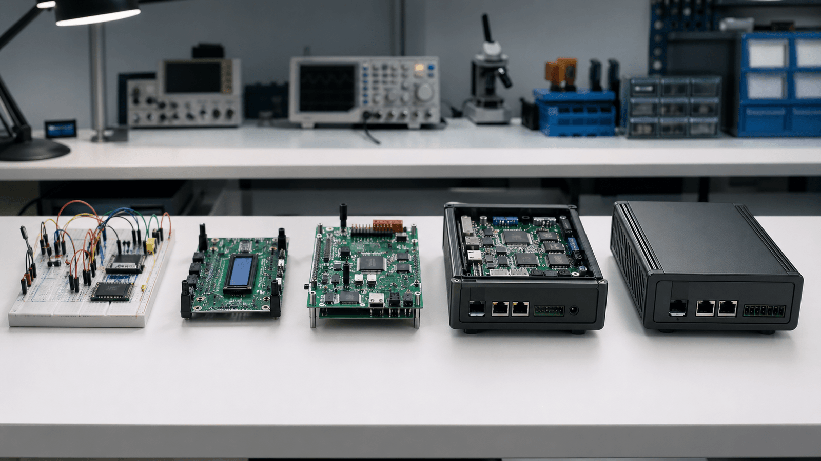
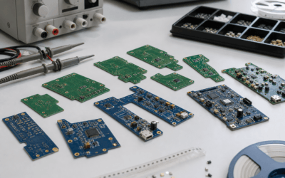
Stage 5 – Prototyping and Validation
Prototyping produces working hardware that can be tested against the original requirements. A well-resourced electronics development programme typically runs multiple prototype iterations – proof-of-concept (PoC) first, then engineering validation (EVT), design validation (DVT), and production validation (PVT) – each with progressively tighter tolerances and more complete firmware.
Quick-turn prototyping services compress the time between board design and physical hardware in hand from weeks to days. Zeus Design’s rapid electronics and PCB prototyping service supports early-stage PoC builds through to functional prototypes used for pre-compliance testing and investor demonstrations.
Deliverables: assembled prototype boards, test reports, firmware build, issue log for design revision.
Stage 6 – Compliance and Certification
In Australia, most electronics products sold to consumers or businesses must carry the RCM (Regulatory Compliance Mark), which covers electrical safety and electromagnetic compatibility (EMC). Products connecting to the public telecommunications network require additional ACMA approval. Exported products may also require CE marking (EU), FCC authorisation (USA), or UKCA marking (UK), each with their own test standards and documentation requirements.
Compliance testing against standards such as AS/NZS CISPR 32, AS/NZS 4268, and IEC 62368-1 is conducted at accredited test laboratories. Pre-compliance testing – conducted on prototype hardware before formal submission – is the most effective way to identify and correct failures before the cost of a formal test run has been committed. Design choices at the schematic and PCB layout stages have a direct and large effect on EMC test results; compliance cannot be treated as a bolt-on activity. The ACMA publishes full guidance on the RCM scheme for Australian suppliers.
Deliverables: pre-compliance test report, EMC remediation actions, formal test reports, declaration of conformity, RCM label artwork.
Stage 7 – Design for Manufacture (DFM)
DFM is the process of reviewing and modifying the electronics design to ensure it can be assembled, tested, and produced reliably at the target volume and cost. DFM covers component package selection, pad geometry, solder mask relief, fiducial placement, panelisation, test point accessibility, conformal coating windows, and rework access. A product that passes functional testing but fails DFM review will encounter yield problems, elevated defect rates, and inflated assembly costs at scale.
DFM should be an ongoing consideration from the schematic stage, not a single review gate before production release. IPC standards (particularly IPC-2221 for PCB design and IPC-A-610 for acceptability of assemblies) provide the industry baseline that contract manufacturers assess boards against.
Deliverables: DFM report, updated PCB design files, revised BOM with approved alternates, assembly instructions.
Stage 8 – Production Handover
Production handover packages all technical documentation required by a contract manufacturer (CM) to produce the product without further engineering input: Gerber files, drill files, BOM with manufacturer part numbers and approved alternates, assembly drawings, test specifications, firmware programming instructions, and acceptance test criteria. A well-prepared production package reduces NRE (non-recurring engineering) charges at the CM and minimises the risk of production holds while engineering questions are resolved.
Deliverables: complete production package, test jig specifications, firmware flashing procedure, first-article inspection (FAI) criteria.
Key Risks at Each Stage and How to Manage Them
Most electronics development failures are predictable. The following risks recur across projects regardless of team experience or product type.
Requirements Creep
Scope additions after design has begun are the most common cause of timeline blowouts. Every new feature or changed requirement after schematic sign-off generates rework across schematic, layout, firmware, and potentially compliance. Manage this with a formal change control process and a requirement freeze date before PCB layout begins.
Component Availability
The global electronics supply chain remains vulnerable to allocation events, long lead times, and end-of-life notices. Microcontrollers, power management ICs, and wireless modules are frequent problem areas. Mitigation includes multi-sourcing critical components during architecture selection, maintaining an approved alternates list on the BOM, and avoiding sole-source components wherever feasible. AusIndustry’s emerging technology resources include guidance on supply chain resilience for Australian manufacturers.
EMC Failure at Pre-Compliance
Electromagnetic compatibility failures discovered at formal test are expensive – both in test laboratory fees and in the engineering time required to diagnose and remediate conducted or radiated emissions. EMC-aware schematic and layout practices, pre-compliance testing on prototype hardware, and early engagement with a compliance engineer are the standard mitigation strategies.
Firmware and Hardware Integration Gaps
When firmware development begins after hardware is finalised, integration issues surface late – at the validation prototype stage – when they are expensive to resolve. Running hardware and firmware development concurrently, with a shared interface specification document, reduces this risk significantly. Zeus Design’s embedded software development capability operates alongside the hardware team for this reason.
DFM Issues Discovered at Production
DFM problems found after tooling is committed – tombstoning, bridging, insufficient test point access, panel routing stress fractures – generate yield losses and rework costs that erode margin. The mitigation is conducting a formal DFM review with the intended CM before releasing production files, not after the first production run reveals the issues.
Cost Drivers in Electronics Development
Electronics development costs are driven by a combination of engineering complexity, iteration count, compliance requirements, and production volume. The following factors have the largest effect on total project cost.
Design Complexity
Layer count, component density, high-speed interfaces, RF circuitry, analog signal chains, and power management complexity all increase engineering time. A four-layer general-purpose microcontroller board costs substantially less to design and lay out than a twelve-layer mixed-signal board with multiple high-speed serial interfaces and an integrated RF front end.
Number of Prototype Iterations
Each prototype spin carries fabrication, assembly, and component costs plus the engineering time to review, diagnose, and revise. Thorough upfront design review and simulation reduce the number of spins required. Industry norms for a moderately complex product are two to four prototype iterations before production release.
Compliance Scope
Each additional regulatory mark – FCC, CE, UKCA, KC, MIC – adds formal test costs, documentation, and potentially additional pre-compliance iterations. Products targeting multiple markets should plan compliance costs per market from the architecture stage. Standards Australia maintains the current applicable standard sets for Australian market entry.
Component Costs and BOM Optimisation
BOM cost at volume is directly affected by component selection decisions made during architecture and schematic stages. Commodity components with multiple approved sources cost less and are more resilient than specialist or sole-source devices. BOM optimisation – substituting equivalent components with better price or availability characteristics – is most effective before PCB layout is finalised, because some substitutions require layout changes.
NRE Versus Unit Cost Trade-offs
High non-recurring engineering (NRE) investment in DFM, automated test fixtures, and production tooling reduces per-unit manufacturing cost and defect rates. At volumes above a few hundred units, this trade-off typically favours the NRE investment. At very low volumes, minimising NRE and accepting higher unit cost is often the commercially rational choice. Engineers Australia publishes resources on engineering project cost estimation and commercial decision frameworks relevant to Australian product development teams.
Zeus Design’s Electronics Development Process and Deliverables
Zeus Design provides end-to-end electronics development from its Sydney-based team, covering every stage from requirements definition through to production handover. The process is structured to give clients clear visibility at each stage gate, with fixed deliverables and a single point of accountability rather than a fragmented contractor model.
The Zeus Design electronics development workflow includes:
- Requirements and architecture review – working with the client team to define functional requirements, select the system architecture, and identify compliance pathways before design begins.
- Schematic design and design review – full schematic capture with integrated DFM and EMC considerations, followed by formal design review before PCB layout begins.
- PCB layout and signal integrity – multilayer PCB design using Altium Designer, with impedance-controlled routing, EMC-aware layout, and DFM rule checking throughout.
- Rapid prototyping – quick-turn PCB fabrication and assembly for proof-of-concept, EVT, and DVT builds, with component sourcing managed by Zeus Design.
- Embedded firmware development – concurrent firmware development integrated with hardware validation, covering boot sequences, peripheral drivers, communication stacks, and application logic.
- Compliance support – pre-compliance test coordination, EMC remediation, and documentation preparation for RCM, CE, FCC, and other applicable marks.
- DFM review and production package – formal DFM review with the production CM, BOM finalisation with approved alternates, and complete production documentation.
Zeus Design’s full electronics design service page details the complete scope of deliverables and the types of products the team has designed for Australian and international clients.
How Electronics Development Connects to Related Services
Rapid Prototyping
Quick-turn prototyping is not a standalone service – it is an integral part of the development lifecycle. Getting hardware into test earlier, more frequently, and at lower cost per iteration is the single biggest process improvement available to most hardware product teams. Zeus Design’s rapid electronics and PCB prototyping service is designed to compress the design-build-test cycle from weeks to days, keeping development momentum and reducing the cost of late-stage discovery.
Embedded Software and Firmware
Electronics development that treats firmware as an afterthought consistently underperforms. Firmware complexity has increased sharply as products have become connected, security-sensitive, and field-updateable. Running firmware development concurrently with hardware – with shared hardware abstraction layers and clear interface specifications – reduces integration risk and allows software testing to begin on hardware earlier in the programme. Zeus Design’s embedded software development service operates as part of the hardware team, not separately from it.
Design for Manufacture
DFM is not a review at the end of development – it is a design philosophy applied throughout. Component package choices, PCB stack-up decisions, footprint standards, and test point placement all affect manufacturing yield and cost. Engaging DFM thinking from the schematic stage, rather than treating it as a pre-production gate, consistently produces better outcomes on unit cost, yield, and time to production release.
FAQs
How long does electronics development typically take from concept to production?
A typical moderately complex electronics product takes between 9 and 18 months from requirements definition to production release. Simple products with standard compliance requirements and few prototype iterations can be done in 6 months. Products with novel RF designs, medical-grade compliance, or complex custom software may take 18 to 24 months or longer. The largest variable is the number of prototype iterations required before the design passes validation.
What does electronics development cost in Australia?
Electronics development project costs vary widely based on complexity and scope. A simple IoT sensor with one wireless interface and standard compliance might cost $30,000-$80,000 in engineering fees. A complex multi-board industrial system with custom enclosure, multiple compliance marks, and embedded software may exceed $250,000. Component and prototyping costs are additional. The most reliable way to get an accurate estimate is a scoped requirements review before quoting begins.
When should I start thinking about compliance?
Compliance planning should begin at the architecture stage – before schematic design starts. The regulatory marks your product will need (RCM for Australia, FCC for the USA, CE for Europe) directly affect circuit design choices, particularly for wireless products and switching power supplies. Products designed without compliance awareness routinely fail pre-compliance testing and require costly redesigns to pass. Early engagement with compliance is always cheaper than late remediation.
What is DFM and why does it matter for my project?
Design for Manufacture (DFM) is the practice of designing electronics so they can be reliably assembled, tested, and produced at scale. DFM affects component package selection, PCB footprint standards, solder paste apertures, fiducial placement, and test point access. Products that pass functional testing but fail DFM review encounter yield problems and elevated rework costs in production. Integrating DFM from the design stage rather than as a late-stage review consistently reduces production cost and improves reliability.
Do I need a local Australian electronics development partner or can I use offshore firms?
Offshore electronics development firms can offer competitive pricing, but they introduce communication overhead, time zone latency, IP transfer risk, and reduced accountability that many Australian product teams underestimate until a project is in trouble. Local partners offer faster iteration cycles, face-to-face design reviews, clearer contractual accountability, and familiarity with Australian compliance requirements. For products with short development windows, complex requirements, or significant IP value, a local partner typically delivers better commercial outcomes despite higher day rates.
What is the difference between a proof of concept and an engineering validation prototype?
A proof of concept (PoC) is a quick, low-cost build that validates core functionality – it does not need to look like the final product or meet all requirements, it just needs to demonstrate that the key technical approach works. An engineering validation prototype (EVT) is a more complete build against the actual schematic and layout, used to validate circuit performance, firmware integration, and preliminary compliance. Most electronics development programmes move through PoC, EVT, DVT (design validation), and PVT (production validation) in sequence, with each iteration closer to the final production configuration.
Can Zeus Design manage both the electronics hardware and the embedded software?
Yes. Zeus Design provides concurrent hardware and embedded software development as a single integrated service. The hardware and firmware teams share interface specifications from the outset, firmware testing begins on prototype hardware as early as the EVT stage, and production firmware is validated alongside the final DFM review. This eliminates the integration gaps that commonly arise when hardware and software development are contracted separately to different teams.
Start Your Electronics Development Project
Whether you are moving a concept toward feasibility, an early prototype toward production, or an existing product through compliance and DFM – Zeus Design’s Sydney-based team provides the full spectrum of electronics development services under one roof. Talk to us about your project and we will give you a clear scope, timeline, and cost estimate with no obligation.
")


0 Comments