
A professional PCB layout service transforms a validated schematic into a board file that can be reliably manufactured, tested and scaled. This guide is written for hardware founders, product managers and engineering teams who need to understand what that process involves, where the risk sits and what to look for in a design partner. We cover layer stack-up decisions, signal integrity, EMC-aware routing, design-for-manufacture review and how Zeus Design approaches each stage.
TL;DR
- PCB layout is the step between a verified schematic and a Gerber file your contract manufacturer can build – it is not simply “drawing traces”.
- Stack-up selection determines layer count, impedance control, power distribution and EMC performance before a single trace is placed.
- Signal integrity and EMC-aware routing are engineering decisions made during layout – they cannot be corrected cheaply after fabrication.
- A DFM review integrated into layout reduces assembly yield failures and redesign cycles before production.
- Deliverables from a quality PCB layout service include Gerber files, ODB++, BOM, assembly drawings, IPC netlists and a DFM sign-off report.
- Zeus Design provides end-to-end circuit board design and layout as part of its electronics design service – covering schematic-to-layout handover, stack-up planning, SI analysis and production file generation.
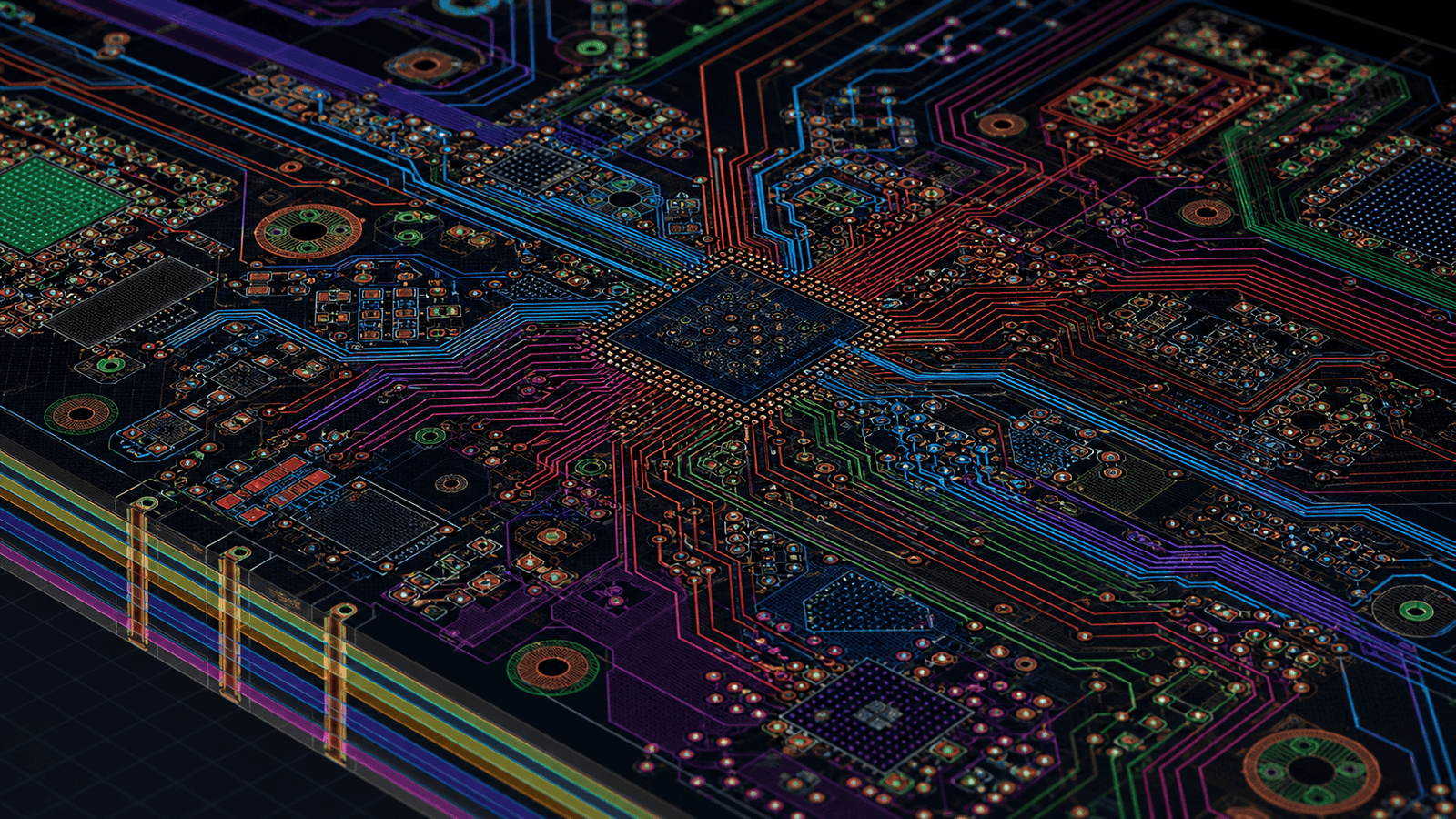
Why PCB Layout Is More Than Placing Components
Most non-engineers assume PCB layout is a drafting task – take the schematic, place the parts, draw the connections. In practice, layout is where a significant share of hardware risk is resolved or locked in. A board that passes simulation and works on a prototype bench can still fail EMC certification, suffer marginal timing margins at temperature, or produce poor assembly yield if the physical design decisions were made carelessly.
Product teams engaging a PCB layout service for the first time often underestimate scope because the schematic already exists. The schematic defines what the circuit does electrically. Layout defines how it behaves physically – and physical behaviour governs signal quality, thermal management, electromagnetic emissions, and whether a CM can assemble the board at acceptable yield.
The gap between a schematic that works in simulation and a PCB that passes compliance testing is filled by layout decisions. Understanding what a professional layout service actually covers helps you scope engagements correctly, brief designers effectively and avoid the expensive redesign cycles that follow under-specified layout work.
What a PCB Layout Service Covers
Schematic Review and Design Rule Setup
A thorough layout engagement starts with a schematic review before any component is placed. Layout engineers check for errors the schematic stage routinely misses – missing decoupling capacitors, incorrect footprint assignments, power rail ambiguities, net naming inconsistencies and component library mismatches. Catching these early avoids mid-project disruption and unplanned redesign cycles.
Alongside schematic review, the designer configures design rules: minimum trace widths and spacings, via constraints, copper pour rules, component keep-out zones, and controlled impedance targets. These rules are enforced throughout the layout by the PCB design tool – in professional engagements, Altium Designer is the dominant platform used by Australian electronics design houses, and its rules-driven engine enforces constraints in real time as routing proceeds.
Layer Stack-Up Selection
Stack-up is one of the most consequential decisions in PCB layout. The arrangement of signal layers, power planes and ground planes determines impedance control accuracy, EMI suppression, crosstalk management and manufacturing cost. A 4-layer board produces significantly lower radiated emissions than an equivalent 2-layer design – published field studies cite reductions of around 15 dB when a continuous ground plane sits immediately adjacent to a signal layer.
A quality PCB layout service selects stack-up based on several factors:
- Signal speed and frequency content – high-speed digital interfaces (USB 3.x, PCIe, GbE, DDR) require reference planes close to signal layers and may need controlled differential impedance.
- Power distribution requirements – boards with multiple power domains benefit from dedicated power planes to minimise resistive drop and distribute decoupling effectively.
- EMC targets – compliance certification requirements (CE, FCC, RCM for Australian/NZ markets) influence stack-up choices before routing begins.
- Board thickness and fabrication capability – the target CM’s process capabilities constrain minimum dielectric thickness, aspect ratio on vias, and copper weight options.
For most IoT and industrial products, a 4-layer stack-up (signal – ground – power – signal) is the minimum that supports reliable high-speed operation. More complex mixed-signal boards, RF designs or high-density interconnect (HDI) applications may require 6, 8 or more layers. Altium’s stackup documentation provides a practical reference for how these decisions are managed in a modern design environment.
Component Placement
Placement is the part of PCB layout that most directly influences both signal integrity and assembly yield. Placement decisions include:
- Grouping components by function – keeping high-speed signal paths short by co-locating their critical components.
- Decoupling capacitor positioning – bypass caps must be placed as close as possible to the power pins they serve, with vias to the power plane directly under or adjacent to the pad.
- Thermal management – power dissipating components need adequate copper area or thermal relief to prevent localised heating that degrades reliability.
- Mechanical constraints – connectors, mounting holes, display cut-outs, antenna keep-outs and user-accessible interfaces must align with the enclosure design.
- Assembly process compatibility – single-sided versus double-sided population, SMT reflow profile requirements, and wave-solder exclusion zones all affect placement decisions.
A placement that satisfies EMC and SI requirements but ignores assembly process requirements creates yield problems at the CM. Professional layout integrates both perspectives from the start.
Signal Integrity and Controlled Impedance Routing
Signal integrity (SI) covers the fidelity with which high-speed signals propagate from driver to receiver. Degraded SI manifests as timing failures, increased bit error rates, or functional instability that is hard to diagnose in field returns. The root causes are physical: trace impedance mismatch, reflections from discontinuities, crosstalk between parallel conductors, or broken reference plane continuity.
A PCB layout service addressing signal integrity will:
- Calculate controlled impedance targets for each high-speed net class and configure them in the design rules.
- Route differential pairs with matched lengths and consistent spacing to maintain impedance throughout.
- Minimise via transitions on high-frequency nets and add back-drill or anti-pad geometry where stub reflections are a concern.
- Apply length matching and propagation delay constraints to parallel bus interfaces such as DDR memory.
- Maintain unbroken reference plane continuity under high-speed signal routes – gaps in the reference plane force the return current to find an alternate path, creating a loop antenna and degrading both SI and EMC.
Altium’s high-speed design documentation covers the design rules and interactive routing constraints used to manage these requirements in production layouts.
EMC-Aware Routing
Electromagnetic compatibility – ensuring the product neither emits beyond regulatory limits nor is disrupted by external interference – is substantially determined by layout. Fixing EMC at the layout stage costs a fraction of what remediation costs after a failed pre-compliance or compliance test.
EMC-aware layout practices include:
- Return current path management – keeping return currents close to their signal paths minimises loop area and therefore radiated emissions.
- Ground plane integrity – avoiding splits or slots in ground planes under high-frequency traces; where splits are necessary (mixed-signal designs), manage the boundary carefully.
- Filtering at board boundaries – placing EMI filter components (ferrite beads, capacitors, common-mode chokes) at cable entry and exit points, with short traces from the filter to the connector.
- Clock and oscillator placement – high-frequency clocks are routed short and shielded from sensitive analogue sections and external connectors.
- Isolation barriers – galvanic isolation circuits (optocouplers, digital isolators) require careful partitioning of primary and secondary grounds.
For products sold in Australia and New Zealand, compliance with the ACMA technical standards and the RCM mark requirements means EMC performance has direct commercial consequences. An EMC-unaware layout reaching pre-compliance testing is an expensive place to discover structural problems.
Power Distribution Network Design
The power distribution network (PDN) delivers clean, stable supply voltage to every component under all operating conditions. A weak PDN causes noise on sensitive analogue circuits, microcontroller resets during load transients and RF performance loss on wireless modules.
PDN-aware layout covers bulk and high-frequency decoupling capacitor sizing and placement, power plane impedance optimisation for target frequency ranges, and via stitching to maintain low-impedance current paths through the power hierarchy. For products with switching regulators, the hot loop between switch, diode and inductor demands careful layout to contain EMI from the high di/dt switching current.
DFM Review
Design for manufacture (DFM) review during or after layout identifies features in the board design that will cause problems during fabrication or assembly. Common DFM issues include:
- Copper-to-board-edge clearances too small for the target fabricator’s process.
- Via drill-to-copper ratios outside the fabricator’s aspect ratio capability.
- Pad sizes or solder mask openings inconsistent with the assembly house’s paste stencil aperture guidelines.
- Component courtyard overlaps that prevent simultaneous placement during pick-and-place.
- Absence of test points for in-circuit test or bed-of-nails test access.
- Fiducial marker placement insufficient for vision-based alignment during SMT assembly.
DFM review standards are often benchmarked against IPC-2221 (generic PCB design standard) and IPC-A-610 (acceptability of electronic assemblies). A layout that passes DFM review before Gerber release reaches the CM in a state where first-article builds are likely to succeed.
When a Project Needs a Dedicated PCB Layout Service
Not every board needs a specialist layout engagement. A simple 2-layer board with a microcontroller, a handful of passives and no high-speed interfaces can often be handled by the circuit designer. The need for a dedicated layout service scales with complexity:
- Signal frequency and data rate – anything above 100 MHz on the PCB, or interfaces like USB 2.0/3.x, MIPI, GbE, DDR3/4 or PCIe benefits from SI-aware layout.
- Layer count – 4-layer and above designs with multiple power domains and controlled impedance requirements.
- Mixed-signal designs – boards combining high-frequency digital circuits with precision analogue measurement, audio, or RF.
- Compliance targets – any product needing CE, FCC, RCM or equivalent certification where EMC layout is a primary lever.
- Production volume – higher-volume products where yield and test access must be engineered in at layout stage.
- Tight mechanical envelope – wearables, industrial sensors or products where the PCB must fit a specific form factor with high component density.
If your product sits in two or more of these categories, a dedicated PCB layout service is not overhead – it is risk reduction.
Technical and Commercial Risks to Manage
Schematic-Layout Mismatch
A schematic not reviewed for layout implications can contain net assignments, component choices or topology decisions that create avoidable complexity. The classic example: a component selected for its electrical characteristics but with a footprint that requires tight-pitch routing the target CM cannot reliably assemble. Resolving this during schematic review costs next to nothing. Resolving it after layout is complete costs a partial redesign.
Compliance Failure After First Build
Pre-compliance or full compliance failures after a first build are expensive – in testing fees and in the redesign and re-spin cycle that follows. Most EMC failures trace back to layout: inadequate ground plane continuity, poor filtering placement, unshielded clock traces or unintentional antenna structures from discontinuous return paths. These are layout problems, not schematic problems – and they are rarely caught until a physical board is tested.
Assembly Yield and Rework Cost
A layout that has not gone through DFM review often produces avoidable first-article defects: tombstoned 0402 resistors from unequal thermal pad geometry, bridging on fine-pitch QFN components from insufficient solder mask web, or alignment drift on large panels from missing fiducials. Each rework incident adds cost and slips the production schedule.
Intellectual Property
PCB Gerber files and design source files are the physical implementation of your product IP. Before signing, confirm the NDA and IP assignment terms: who owns the source files, what the retention policy is, and what use restrictions apply after the engagement concludes.
Zeus Design’s Circuit Board Design and Layout Service
Zeus Design provides circuit board design and PCB layout services as a core engineering capability – from simple 2-layer boards through to complex multilayer, high-speed and mixed-signal designs for Australian product teams and hardware startups.
The layout service integrates directly with Zeus Design’s electronics design capability. Schematic design, layout and firmware development are handled by a single team, which removes the handover friction that arises when these stages are split across different providers. The engineers who understand the circuit’s intended behaviour are the same ones ensuring the layout preserves it.
Typical deliverables from a Zeus Design PCB layout engagement include:
- Reviewed and updated schematic files.
- Completed PCB layout source files (Altium Designer format).
- Gerber and drill files ready for fabrication.
- ODB++ files where the target CM requires them.
- BOM with approved manufacturer part numbers and alternates.
- Assembly drawings and pick-and-place centroid files.
- DFM review report against the target CM’s process capabilities.
- Stack-up specification with controlled impedance targets for the fabricator.
For products requiring compliance certification, the layout process incorporates the EMC design practices that reduce compliance risk – return path management, filtering placement, ground plane continuity, and antenna isolation – before the first board is built. This is integrated alongside rapid prototyping services that get a functional board in hand quickly for validation.
How PCB Layout Connects to Related Services
PCB layout sits at the centre of a broader product development workflow. Understanding the upstream and downstream connections helps product teams plan engagements and avoid the cost of disconnected handovers.
Upstream: Schematic and Circuit Design
Layout quality depends on schematic quality. A schematic designed with layout in mind – considering decoupling strategy, power sequencing, differential pair assignments and impedance-sensitive topology choices – produces a cleaner layout with fewer iterations. Zeus Design’s electronics design service covers schematic design through to layout as an integrated engagement.
Downstream: Prototyping and Validation
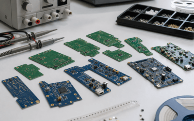
A completed layout feeds directly into PCB fabrication and assembly. Zeus Design’s rapid prototyping service manages fabrication and assembly of prototype boards from the Gerber and BOM output of the layout stage, including first-article inspection and functional test support.
Firmware and Hardware Co-Development
Hardware and firmware developed in parallel reduce total development time and improve functional validation coverage. Zeus Design’s embedded software development service works alongside PCB layout and prototyping so firmware bring-up can begin as soon as prototype boards are assembled.
FAQs
What does a PCB layout service actually deliver?
A PCB layout service delivers the physical design files needed to fabricate and assemble a printed circuit board from a schematic. Deliverables typically include Gerber fabrication files, drill files, a BOM with approved part numbers, assembly drawings, pick-and-place centroid files, and a DFM review against the target manufacturer’s capabilities. Some engagements also include a stack-up specification document and controlled impedance targets for the fabricator.
How many layers does my PCB need?
Layer count depends on signal complexity, frequency, power domain count and EMC requirements. A simple low-speed board with one power domain can often work on 2 layers. Any product with high-speed digital interfaces (USB, GbE, DDR, PCIe), RF content, or multiple isolated power domains typically warrants at least 4 layers. Mixed-signal, high-density or compliance-critical designs often need 6 or more. Your PCB layout designer should recommend a stack-up based on your specific design requirements, not a default preference.
What is signal integrity and why does it matter for PCB layout?
Signal integrity refers to the fidelity of electrical signals as they travel through the board. Poor signal integrity causes timing failures, data corruption and functional instability that can be difficult to diagnose without a hardware background. It is primarily determined by layout decisions – trace impedance, differential pair matching, reference plane continuity and via geometry. Signal integrity problems discovered after fabrication are expensive to fix because they require a board re-spin.
How does a PCB layout service support EMC compliance?
EMC compliance for CE, FCC and RCM certification is substantially governed by PCB layout. A layout-aware EMC approach includes managing return current paths to minimise loop area, maintaining continuous ground planes under high-frequency traces, placing filtering components correctly at board boundaries and isolating clock and switching signals from sensitive circuits. Addressing EMC at layout stage costs a fraction of the pre-compliance test failure, redesign and re-test cycle. See Zeus Design’s electronics design service for compliance-integrated layout support.
What is DFM review and when should it happen in the layout process?
DFM (design for manufacture) review checks that the PCB layout is compatible with the fabrication and assembly processes of your target contract manufacturer. It covers clearances, via aspect ratios, pad geometry, solder mask rules, fiducial placement and test point access. DFM review should happen before Gerber release – ideally as an integrated step in layout rather than a separate post-layout check – so that issues are corrected before the design is submitted for fabrication.
What file formats does a PCB layout service typically provide?
Standard deliverables include Gerber RS-274X files and Excellon drill files for fabrication, ODB++ format where required by the CM, a CSV or XLS BOM with manufacturer part numbers and quantities, pick-and-place centroid files for SMT programming, and PDF assembly drawings. Source files in the design tool format (commonly Altium Designer) are also provided in professional engagements, allowing the client to own and modify the design independently.
Can Zeus Design take over a PCB layout from another designer?
Yes. Zeus Design can import and work with designs started by another team, provided source files are available in Altium Designer format or a transferable format. The engagement typically begins with a design review to assess the current state, identify any schematic or placement issues, and agree on the scope of work to bring the layout to production-ready standard. For more detail, see the circuit board design service page.
Conclusion
A PCB layout service is the bridge between a verified schematic and a board that can be manufactured reliably, pass compliance testing and scale to production without expensive redesign. The work spans stack-up selection, signal integrity, EMC-aware routing, power distribution and DFM review – each stage reducing risk that would otherwise surface as a costly failure downstream.
For product teams and hardware startups, layout is not a commodity task to be minimised. It is where hardware risk is either managed or deferred. Engaging a layout service that understands the full chain – from schematic intent through to CM process requirements – is one of the most direct ways to compress your development timeline and reduce first-build surprises.
Zeus Design provides circuit board design and PCB layout as part of an integrated electronics design engagement. If you have a schematic ready for layout, or a project where schematic and layout need to be developed together, contact Zeus Design to discuss scope and timeline.
")


0 Comments