
This guide examines what comprehensive electronics engineering solutions actually cover for product companies with demanding hardware requirements – including signal integrity, regulatory compliance, and production test systems. It is written for founders, engineering managers, and product teams who are scoping a hardware project and need to understand what a capable design partner should bring to the table, and where the gaps in simpler service offerings tend to appear.
TL;DR
- Electronics engineering solutions for complex hardware go well beyond circuit layout – they span signal integrity analysis, DFM, compliance strategy, and test system design.
- Signal integrity problems (impedance mismatch, crosstalk, EMI) are responsible for a large share of late-stage hardware failures and costly board respins.
- Compliance should be designed in from the start – retrofitting EMC or safety requirements after prototyping is expensive and often forces architecture changes.
- Production test jigs are a non-negotiable part of scaling – without them, yield and quality control become guesswork.
- A capable partner handles electronics design, PCB layout, embedded software, compliance planning and test fixture development under one engagement, so problems do not fall between handoffs.
- Zeus Design delivers end-to-end electronics engineering across these disciplines from its Australian base.
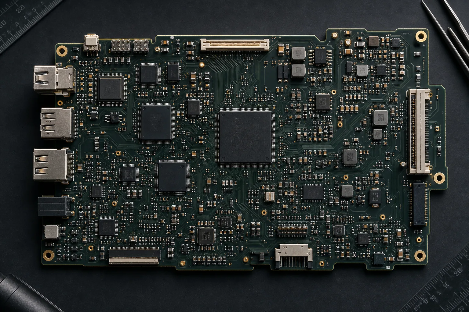
Why Complex Hardware Projects Need More Than PCB Layout
Most product companies begin their hardware journey expecting to commission a PCB design and end up with a working product. In practice, a circuit board is one output of a much larger engineering system. By the time a product reaches production, the team has had to navigate component selection, signal integrity trade-offs, thermal management, electromagnetic compatibility, regulatory submission, and a test strategy that can keep defect rates low at volume.
This is the scope that separates a basic PCB layout service from genuine electronics engineering solutions. Founders and product teams who do not account for this full scope early often find themselves managing multiple specialist contractors, resolving conflicting advice, and absorbing the cost of redesigns that could have been avoided with better upfront engineering.
The projects where this gap is most costly tend to share common traits:
- High-speed digital interfaces (USB 3.x, PCIe, Gigabit Ethernet, MIPI) where signal quality has tight tolerance requirements.
- Wireless or RF-adjacent hardware where unmanaged EMI creates both performance and compliance problems.
- Medical, industrial or safety-relevant devices where regulatory certification is mandatory and cannot be added as an afterthought.
- Products intended for production volumes where test coverage directly affects yield and warranty cost.
The sections below break down what each of these disciplines requires and how they connect to each other in a well-run project.
What Electronics Engineering Solutions for Complex Hardware Include
Signal Integrity Analysis and High-Speed PCB Design
Signal integrity (SI) is the discipline of ensuring that digital and analogue signals travel through a PCB reliably – with acceptable timing, voltage levels, and noise margins at the receiver. As clock speeds increase and board densities tighten, SI problems become the primary cause of intermittent failures, EMC pre-compliance failures, and board respins.
The main failure modes to design against include:
- Impedance mismatch – reflections from unterminated or poorly matched transmission lines that corrupt signal edges and cause logic errors.
- Crosstalk – capacitive and inductive coupling between adjacent traces that introduces noise onto otherwise clean signals.
- Power delivery noise – ground bounce and supply ripple that shifts switching thresholds and causes timing violations.
- EMI from fast-switching traces – high-frequency current loops that radiate and create compliance problems.
Addressing SI properly requires controlled-impedance stackup design, careful routing of high-speed nets, placement of bypass capacitors close to switching loads, and simulation or pre-compliance measurement before final layout sign-off. The Altium constraint-driven PCB design documentation is one useful reference for how these constraints are managed in modern toolchains.
Zeus Design’s circuit board design service covers multilayer PCB layout with EMC-aware design practices, controlled impedance, and signal integrity considerations as part of standard scope – not as an optional add-on.
Regulatory Compliance and Certification Planning
Compliance is not a tick-box exercise at the end of a project. For most product categories sold into Australia, the EU, or North America, the regulatory framework shapes hardware architecture decisions from the earliest design stages.
The key frameworks most product teams encounter include:
- EMC (electromagnetic compatibility) – conducted and radiated emissions, and immunity, tested against CISPR, IEC 61000 or FCC Part 15 standards depending on target market. In Australia, compliance with the Australian Communications and Media Authority (ACMA) requirements is mandatory for radio and communications devices under the ACMA supplier labelling requirements.
- Safety – for mains-connected or battery-powered consumer and industrial devices, IEC 62368-1 (audio/video, IT and communications technology) or IEC 60335 (household appliances) will apply. Electrical safety compliance in Australia is managed under the Electrical Equipment Safety System (EESS).
- Radio/wireless – any product using Wi-Fi, Bluetooth, cellular, LoRa or other licensed/unlicensed spectrum requires radio frequency (RF) compliance and, in Australia, registration with ACMA.
- Industry-specific – medical devices are regulated by the TGA under the Australian medical device regulatory framework; industrial equipment may need additional certifications for hazardous locations or functional safety (IEC 61508).
The engineering implication is that circuit architecture, PCB layer stackup, enclosure design, and component selection all have compliance consequences. A design partner with compliance experience builds these constraints into the hardware from the start – rather than discovering at pre-compliance testing that a fundamental redesign is required.
Zeus Design’s electronics design service includes compliance-focused hardware design and pre-compliance planning as part of its standard engagement scope.
Design for Manufacture
DFM (design for manufacture) bridges the gap between a working prototype and a product that can be assembled reliably and cost-effectively at volume. The issues that DFM addresses are often invisible in prototype builds – hand-assembled one-at-a-time with expert oversight – but become serious defect sources when production moves to automated assembly lines.
Common DFM issues on complex boards include:
- Component clearances that violate pick-and-place or reflow constraints.
- Pad geometries that cause solder bridging or tombstoning on fine-pitch parts.
- Via placement that prevents in-circuit test (ICT) or flying-probe access.
- Panelisation and board edge restrictions that affect automated handling.
- BOM components with poor or single-source availability, creating production risk.
A DFM review before committing to production tooling typically costs a fraction of what a production-stage rework requires. Zeus Design’s electronics design service includes DFM review as part of production handover preparation, ensuring that layout decisions support reliable volume assembly.
Production Test System Development
A production test system is the hardware and software infrastructure that validates each unit coming off the assembly line before it ships. For complex boards, this is not optional – it is the mechanism that separates defective units from good ones and protects warranty costs.
The two main approaches are:
- In-circuit test (ICT) – uses a bed-of-nails fixture to contact test points on the PCB and verify component values, shorts, and opens. Fast and thorough, but requires test point access on the board and a relatively high fixture cost.
- Functional test jigs – custom fixtures that connect to the board’s external interfaces and run end-to-end functional tests that verify the assembled product behaves correctly. More flexible and lower fixture cost, but requires development of custom test firmware or software.
Zeus Design develops custom test jigs and test fixtures alongside the product hardware, so the test strategy is designed in parallel with the PCB rather than reverse-engineered after the fact. This is a meaningful difference – boards designed without test access in mind often require hardware spins to add test points, adding cost and delay.
For teams new to production test planning, the IPC standards body publishes relevant guidance on test strategy in documents such as IPC-7711/7721, which cover rework and repair – but the core test design principles apply broadly to any volume electronics project.
When a Project Needs Comprehensive Electronics Engineering Solutions
Not every hardware project needs the full scope described above. A simple sensor board with low-speed interfaces and no wireless functionality may be well-served by a straightforward PCB design engagement. The indicators that a project needs broader engineering solutions include:
- High-speed digital interfaces – any interface above around 100 MHz or with strict timing budgets (USB 3.x, MIPI CSI/DSI, PCIe, DDR memory, Gigabit Ethernet) warrants SI analysis as a first-class concern.
- Wireless connectivity – any product using 2.4 GHz, 5 GHz, sub-GHz, or cellular bands will need antenna design, RF layout, and compliance testing. Read more about how Zeus Design approaches this in our IoT device design guide.
- Regulated markets – medical, industrial, safety-critical, or export products where certification is a commercial requirement rather than a best-practice recommendation.
- Production volume above a few hundred units – at this scale, test systems pay for themselves quickly and DFM problems become significant cost drivers.
- Complex firmware or software integration – products where embedded firmware must be co-developed with the hardware to meet performance and reliability requirements.
Technical and Commercial Risks to Manage
Hardware projects at this level of complexity carry a predictable set of risks. Understanding them in advance helps product teams make better decisions about where to invest engineering time and budget.
Late-stage signal integrity failures
SI failures discovered at pre-compliance or certification testing can require partial or complete re-layout. The cost is not just the PCB spin – it is the delay to market, the engineering rework, and the risk that the architecture needs changing. Addressing SI in the initial design phase is significantly cheaper.
Compliance surprises
A product that fails FCC Part 15 or ACMA testing because of EMI from an unshielded switching regulator or a poorly routed high-speed interface may need new board layers, shielding, or topology changes. Pre-compliance testing at a test house during development – before final submission – is standard practice for experienced teams and catches these issues while changes are still manageable.
Component obsolescence and BOM risk
The global components market has demonstrated that single-source or allocation-constrained parts create serious production risk. A hardware engineering partner that includes BOM risk assessment in the design phase – selecting components with multiple qualified sources and healthy inventory – reduces the probability of a production-halting shortage.
Test coverage gaps
Shipping products without adequate test coverage is a bet on your assembly quality. Most contract manufacturers provide basic electrical test (shorts and opens), but functional test of the full application layer requires purpose-built fixtures. Teams that skip this typically see it in warranty return rates.
Zeus Design’s Process and Deliverables
Zeus Design approaches complex hardware projects as an integrated engineering engagement – not a sequence of isolated deliverables handed off between specialists. The typical flow for a complex hardware project looks like this:
- Feasibility and requirements – clarifying the product’s performance requirements, target markets, regulatory obligations, and production volume before design work begins.
- Architecture and component selection – selecting the core silicon, communication interfaces, power topology, and mechanical constraints that will define the design space.
- Circuit design and schematic capture – developing the full circuit schematic with compliance, SI, and DFM constraints already in scope.
- PCB layout – multilayer layout with controlled impedance, EMC-aware routing, and DFM rules applied throughout. Altium Designer is used for all PCB work.
- Prototype build and bring-up – rapid PCB prototyping followed by systematic bring-up, debugging, and validation. See our electronics prototyping guide for more on this phase.
- Firmware and software development – embedded firmware co-developed with the hardware, covering peripheral drivers, communication stacks, application logic, and OTA update infrastructure where required.
- Pre-compliance and compliance testing – pre-compliance testing during development, followed by support for formal submission at an accredited test house.
- Test jig development – custom functional test fixtures developed alongside the hardware and validated before production handover.
- DFM review and production handover – final DFM review, manufacturing documentation package, and production support.
How This Connects to Related Services
Electronics engineering rarely exists in isolation. A hardware product that needs wireless connectivity also needs cloud infrastructure for device management. A medical device needs firmware that satisfies software quality requirements under IEC 62304. An IoT product needs a mobile app for configuration and monitoring.
Zeus Design covers these adjacent layers within a single engagement:
- Embedded software and firmware – developed alongside the hardware to avoid the integration problems that arise when firmware is treated as a separate workstream.
- IoT connectivity – wireless stack integration, secure device provisioning, and cloud-connected architecture for devices that need remote management or telemetry.
- Mobile app development – iOS and Android companion apps built to integrate with the device’s communication interfaces and cloud backend.
- Cloud and backend systems – device management platforms, APIs, and data pipelines for connected products.
This breadth matters because problems at the boundary between hardware, firmware, and software are among the most expensive to diagnose and fix. When the same team that designed the PCB also writes the firmware and the cloud integration, the boundary problems largely disappear.
FAQs
What does “electronics engineering solutions” actually mean in practice?
Electronics engineering solutions refers to the full set of engineering disciplines needed to take a hardware product from concept to production – including circuit design, PCB layout, signal integrity, compliance planning, embedded firmware, and test system development. It is distinguished from a basic PCB layout service by the breadth of engineering judgement applied across the full product development cycle, not just a single deliverable.
How much does signal integrity analysis add to a project?
For straightforward low-speed boards it adds little – SI considerations are handled by good layout practice. For high-speed designs, dedicated SI analysis typically adds a few days of engineering time in the layout phase, but prevents board respins that routinely cost $5,000-$30,000+ in prototype fabrication, assembly, and delay. The return on investment is strong for any product with interfaces above 100 MHz. See Synopsys’s signal and power integrity resources for a technical overview.
When should compliance planning start in a hardware project?
At architecture stage – before schematics are captured. The choice of switching regulator topology, wireless module, connector types and enclosure design all have compliance consequences. Retrofitting EMC or safety compliance requirements after prototyping typically requires partial redesign and adds weeks to months to a project schedule.
Do I need a custom test jig for every product?
For low-volume products (under a few hundred units) a manual test procedure with a standard bench setup may be acceptable. At production volumes, a custom test jig becomes cost-effective quickly – it reduces test time per unit, removes operator variability, and creates a documented, repeatable quality gate. The fixture cost is typically recovered within the first few hundred units tested.
What is the difference between a prototype and a production-ready design?
A prototype validates that the circuit and firmware work. A production-ready design also satisfies DFM requirements for automated assembly, includes test point access for functional testing, has a validated BOM with acceptable lead times and multiple sources, and has passed or is on track for regulatory certification. The gap between the two is often underestimated by teams building their first hardware product.
Can Zeus Design handle the full scope from electronics design through to test jigs and compliance?
Yes. Zeus Design covers the full hardware engineering scope – circuit design, multilayer PCB layout, embedded firmware, compliance planning, test jig development, and DFM review – within a single engagement. This avoids the handoff problems that arise when these disciplines are spread across separate contractors. Contact Zeus Design to discuss your project requirements.
What makes Australian electronics engineering different from offshore alternatives?
Australian regulatory requirements (ACMA, EESS, TGA for medical) have local-specific obligations that an Australian engineering partner understands directly. Proximity also means faster iteration on prototypes, easier in-person collaboration during bring-up and debugging, and a shared business timezone for project management. For products intended for the Australian market, local compliance knowledge is a genuine engineering asset.
Conclusion
Complex hardware projects succeed when the engineering solution covers the full scope – not just circuit design and PCB layout, but signal integrity, compliance strategy, test system development, and the firmware and software layers that make the product work in the field. Treating these as separate problems to be solved later is the primary source of expensive late-stage redesigns and compliance delays.
Zeus Design provides integrated electronics engineering solutions for Australian and international product companies with demanding hardware requirements. Whether you are starting from a concept or rescuing a project that needs more rigorous engineering, the team covers electronics design, PCB layout, firmware, test jig development, and compliance planning as a unified engagement.




0 Comments