
Electronics prototyping is the structured process of converting a product concept into working hardware – and for hardware startups and product teams, how well you manage each prototyping stage determines whether you reach production on budget and on schedule. From a rough proof of concept to a fully functional PCB build ready for design-for-manufacture review, every iteration adds evidence, reduces risk, and sharpens the product definition. Zeus Design works with Australian engineering teams at every stage of this journey, from initial schematic to production-ready boards.
TL;DR
- Electronics prototyping moves through four stages: proof of concept, breadboard/bench prototype, PCB prototype, and functional build.
- Each stage has a different purpose – don’t skip stages to save time; you’ll pay more in rework later.
- Iteration speed and DFM readiness are the two main forces in tension across the prototyping cycle.
- PCB prototyping decisions – layer count, component footprints, signal integrity – made early have outsized impact on production cost and yield.
- Firmware and hardware should be developed in parallel; late firmware integration is one of the most common causes of prototype delays.
- Zeus Design offers rapid PCB prototyping, circuit board design, and embedded firmware as integrated services – not isolated deliverables.
- Starting DFM conversations at the PCB prototype stage, not after, saves significant redesign cost before manufacturing.
Who Needs Electronics Prototyping Services – and Why It Matters
Hardware product development is expensive to get wrong. Unlike software, where a bug fix is a code push, an electronics error can mean scrapping hundreds of boards, re-spinning a PCB layout, or – in the worst case – discovering a fundamental circuit flaw only after tooling has been cut for an enclosure.
Australian hardware teams face an additional constraint: the local electronics manufacturing ecosystem, while capable, is smaller than North American or European markets. Lead times on specialised components can be longer, and finding an engineering partner who understands both the technical and commercial realities of bringing a product to market in Australia is not straightforward.
The teams who benefit most from a structured electronics prototyping process include:
- Hardware startups validating a product concept before committing to tooling or a manufacturing run.
- Product teams at established businesses adding a connected hardware component to an existing product line.
- R&D departments exploring new sensor, wireless, or power management architectures.
- Industrial OEMs replacing legacy hardware with a modern, production-quality design.
In each case, the goal is the same: reach a functional, manufacturable product with as little wasted engineering effort as possible.
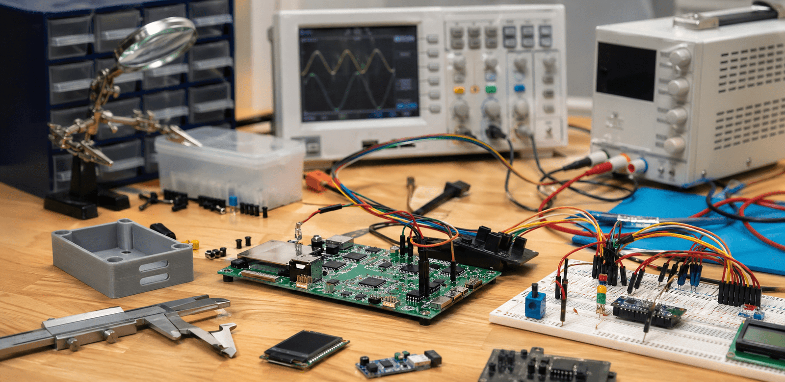
What Electronics Prototyping Actually Involves
A well-run electronics prototyping process is not a single event – it is a sequence of increasingly refined builds, each designed to answer specific questions before moving forward.
Stage 1 – Proof of Concept
The proof of concept (PoC) exists to answer one question: does the core idea work? At this stage, aesthetics, form factor, power efficiency, and manufacturability are deliberately deprioritised. The goal is to validate the fundamental operating principle as cheaply and quickly as possible.
PoC builds typically use development boards (such as Arduino, STM32 Nucleo, or Raspberry Pi compute modules), off-the-shelf breakout boards, and jumper wires. The circuitry is loose and temporary. The firmware is minimal. What matters is that the key function – a sensor reading, a wireless connection, a motor response – is demonstrated on real hardware.
A well-defined PoC saves significant time downstream. If the concept does not work at this stage, the team learns that before investing in PCB design. If it does work, the PoC provides the reference architecture for the next stage.
Stage 2 – Breadboard and Bench Prototype
Moving from a PoC to a breadboard or bench prototype means adding more of the product’s real-world requirements: proper power supply design, real component selections (rather than generic breakout modules), initial EMC awareness, and an interface that reflects the actual product use case.
This stage is where most of the circuit design decisions are made. Microcontroller selection, peripheral interfaces, power rail architecture, and wireless module choices are all locked in at this point. Changes here are inexpensive. Changes after PCB layout has begun are not.
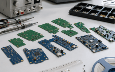
Stage 3 – PCB Prototype
The PCB prototype is the first version of the product’s actual circuit board. This is a significant step – it transforms a collection of bench components into a layout that reflects the real product geometry, connector placement, and assembly process.
PCB prototypes are typically fabricated in small quantities (3-10 boards) and assembled either by hand or by a contract manufacturer. The first PCB spin will almost always have issues: layout problems, signal integrity concerns, component availability constraints, or firmware integration bugs that only surface when running on real hardware. Expecting and planning for at least two PCB spins is prudent engineering practice, not a sign of poor planning.
The IPC-A-610 acceptability standard and its companion IPC-2221 generic PCB design standard provide the industry baseline for what constitutes an acceptable PCB design and assembly – Australian electronics manufacturers and assemblers reference these standards routinely.
Stage 4 – Functional Build
The functional build is a near-production-representative prototype: the PCB layout is stable, the firmware is at feature-complete beta, the enclosure or mechanical interface is finalised (or close to it), and the unit can be tested against real product specifications. This is the stage at which pre-compliance EMC testing, environmental testing, and structured functional validation occur.
A solid functional build is the prerequisite for a meaningful design-for-manufacture review and, ultimately, a production release.
The Core Tension: Iteration Speed vs. DFM Readiness
Every electronics prototyping programme sits on a spectrum between two competing priorities.
Iteration speed favours moving fast, accepting imperfect designs, and learning from real hardware as quickly as possible. It tolerates cost inefficiency and rework in exchange for faster learning cycles. This approach is appropriate in the early stages – PoC and first PCB spin – when the design space is large and the right answers are unknown.
DFM readiness (Design for Manufacture) favours making decisions that will survive contact with manufacturing – component standardisation, panellisation-aware layouts, test point placement, controlled impedance where required, and BOM rationalisation. DFM decisions made late cost significantly more than those made early.
The mistake most teams make is treating these as sequential rather than parallel concerns. A team that focuses exclusively on iteration speed through three PCB spins, then attempts to layer DFM on top at the end, will often find they need a fourth spin purely to address manufacturability. Engineers Australia consistently identifies late DFM integration as a leading driver of product development cost overruns in the electronics sector.
The better approach is to introduce DFM thinking progressively: light DFM awareness at Stage 2, deliberate DFM decisions at Stage 3 (PCB prototype), and a formal DFM review before committing to production tooling.
Managing Prototype-to-Production Risk
The transition from a working prototype to a manufacturable product is where many hardware projects stall. The risks are well-understood but frequently underestimated:
Component Availability and Lifecycle
A component specified during prototyping may be unavailable, discontinued, or subject to minimum order quantities that are impractical for initial production volumes. The global semiconductor supply chain – as demonstrated repeatedly over the past several years – can make components that appeared readily available during prototyping suddenly scarce at production time. Building BOM alternatives into the design from the PCB prototype stage provides resilience.
Yield and Testability
A prototype that works when assembled by a skilled engineer in a lab may not assemble reliably at volume. PCB land patterns, component placement density, and soldermask clearances all affect assembly yield. Test points that seem unnecessary on a hand-assembled prototype become critical when a contract manufacturer needs to run in-circuit tests on every board.
EMC and Regulatory Compliance
In Australia, most commercial electronic products sold or connected to the mains supply require compliance with the ACMA regulatory framework, which incorporates relevant Australian/New Zealand EMC standards. Products with wireless subsystems require ACMA registration. Designing for EMC compliance from the PCB prototype stage – controlled impedance, ground plane continuity, decoupling strategy, enclosure earthing – is far less costly than performing a post-design EMC remediation after failing a test house assessment.
Firmware Maturity
Firmware that is incomplete or untested against real hardware is a common prototype-to-production risk. Hardware bugs and firmware bugs interact in ways that are difficult to isolate when both are evolving simultaneously. Running hardware and firmware development in parallel, with clear interface definitions and early hardware-in-the-loop testing, dramatically reduces integration risk at the functional build stage.
Zeus Design’s Electronics Prototyping Process
Zeus Design’s rapid prototyping service is built around fast, purposeful iterations rather than a single high-stakes prototype. The typical engagement structure for a hardware startup or product team looks like this:
- Requirements and architecture review – Zeus Design reviews the product specification, confirms the technology stack (microcontroller family, wireless protocol, power architecture), and identifies the key unknowns that the PoC needs to resolve.
- Proof of concept build – A working PoC is delivered on development hardware, demonstrating the core product function and de-risking the fundamental technical approach.
- Schematic and PCB layout – Full circuit design and PCB layout are completed using Altium Designer, with DFM and signal integrity considered from the outset. Zeus Design’s circuit board design service covers schematic capture, multilayer layout, EMC-aware routing, and production documentation.
- PCB fabrication and assembly – Prototype boards are fabricated and assembled, with Zeus Design managing the supply chain for components and coordinating with the fabrication house.
- Bring-up and validation – Boards are brought up systematically, power rails verified, firmware loaded, and functional testing conducted against the product specification.
- Iteration and DFM review – Findings from bring-up are fed back into the design. A DFM review is conducted before advancing to the functional build, covering component standardisation, assembly considerations, and test strategy.
How Electronics Prototyping Connects to Related Services
Effective electronics prototyping rarely happens in isolation. The prototype is the starting point for a set of downstream engineering activities, and the decisions made during prototyping directly shape how complex and costly those activities will be.
Circuit Board Design and PCB Layout
The PCB layout is arguably the highest-leverage activity in the entire prototyping cycle. A well-executed layout reduces EMI, improves signal integrity, simplifies assembly, and sets up the product for a smooth DFM review. Zeus Design’s circuit board design service brings Altium Designer expertise and DFM-aware layout practices to every prototype – ensuring that the PCB produced during prototyping is a credible predecessor to the production design, not a throwaway.
Embedded Firmware Development
Hardware without firmware is inert. Zeus Design’s embedded software development capability runs in parallel with hardware design, ensuring firmware is ready to run on prototype boards as soon as they are assembled. This parallel-track approach avoids the common situation where a hardware team finishes a prototype board and then waits weeks for firmware to be written – compressing the overall development timeline significantly.
Full Electronics Design Engagement
For teams who need more than prototyping – who need an end-to-end engineering partner from initial architecture through compliance, DFM, and production handover – Zeus Design’s electronics design service covers the complete product development lifecycle. This includes compliance planning, cost optimisation, test jig development, and manufacturing liaison, delivered as an integrated engagement rather than a series of disconnected handovers.
FAQs
How many prototype iterations should I budget for?
For most new hardware products, budget for at least two PCB spins – a first prototype to validate the design and a revised spin addressing bring-up findings. Complex products involving RF, high-speed digital, or novel power architectures may require three or more iterations. Planning for two spins from the outset leads to better design decisions and more realistic schedules than assuming you will get it right first time.
What is the difference between a proof of concept and a PCB prototype?
A proof of concept uses off-the-shelf development boards and loose wiring to validate a core technical idea as quickly as possible, without regard for form factor or manufacturability. A PCB prototype is a custom-designed circuit board that reflects the real product geometry, component selections, and layout – the starting point for DFM and production planning. Both serve distinct purposes and should not be conflated.
How long does electronics prototyping take in Australia?
A proof of concept can typically be completed in one to three weeks. A first PCB prototype – including schematic, layout, fabrication, and assembly – typically takes four to eight weeks depending on component availability and board complexity. Subsequent iterations are generally faster. Working with an Australian-based design partner such as Zeus Design reduces coordination overhead and time zone friction compared to offshore alternatives.
When should I start thinking about DFM during prototyping?
DFM awareness should begin at the PCB prototype stage, not after. Decisions about component packaging, land pattern standardisation, panellisation, and test point placement made during the first PCB spin are far less expensive to implement than post-prototype rework. A formal DFM review before committing to a production build is strongly recommended regardless of how thorough your prototype DFM process was.
Do I need to have a full specification before starting electronics prototyping?
A complete specification is not required to begin prototyping – in fact, prototyping is often the best way to sharpen an incomplete specification by answering specific technical unknowns through working hardware. What is required is a clear definition of the core function the prototype needs to validate, the target operating environment, and any non-negotiable constraints such as power budget, wireless protocol, or regulatory requirements.
How does Zeus Design handle component sourcing during prototyping?
Zeus Design manages component sourcing as part of the prototyping engagement, drawing on established supplier relationships to source components at prototype quantities. Where components present availability risk, the design team identifies alternatives at the schematic stage – before layout is committed – to avoid last-minute substitutions that can require PCB respins. BOM resilience is treated as a design requirement, not an afterthought.
Can Zeus Design help with EMC compliance from the prototype stage?
Yes. Zeus Design incorporates EMC-aware design practices – controlled impedance, ground plane strategy, decoupling placement, and cable/connector earthing – from the PCB layout stage. For products requiring ACMA registration or international certification (CE, FCC), pre-compliance planning is introduced during the functional build phase, significantly reducing the risk of failing a formal test house assessment and requiring a costly board respin.
Start Your Electronics Prototyping Project
Whether you are validating a concept for the first time or preparing an existing prototype for production, Zeus Design’s team can help you move faster with less risk. From proof-of-concept builds and PCB design through to embedded firmware and DFM review, every stage of your prototyping programme is covered by engineers who understand the Australian hardware market.
")


0 Comments