
A professional circuit board design service covers far more than placing components and routing copper – it is an engineering discipline that spans component selection, schematic capture, multilayer stack-up, signal integrity, EMC-aware layout, design for manufacture and production-ready output. For Australian hardware teams building connected devices, industrial equipment or consumer electronics products, choosing the right circuit board design partner directly affects whether a product reaches production on time and on budget. This guide explains what a complete service covers, how to evaluate providers, and how Zeus Design supports hardware teams across Australia.
TL;DR
- A circuit board design service should cover component selection, schematic capture, multilayer PCB layout, EMC-aware routing, DFM review and a complete production output package.
- Component selection and schematic quality set the ceiling for PCB performance – layout cannot fix a flawed circuit.
- Multilayer stack-up design is a primary EMC and signal integrity control mechanism, not a fabrication afterthought.
- DFM review is the highest-return deliverable for teams approaching first-article fabrication – it prevents yield loss before a board is built.
- Australian circuit board design services offer RCM regulatory familiarity, time-zone access and direct collaboration that offshore providers rarely match on complex projects.
- Zeus Design works in Altium Designer and delivers complete production output packages with native project files retained by the client.
- Integrating firmware development alongside PCB design – rather than sequencing them – reduces hardware-software integration risk and shortens time to validated prototype.
Who Needs a Circuit Board Design Service
Hardware teams reach for an external circuit board design service in three distinct situations. The first is capability gap: the team has strong product and systems engineering depth but lacks a specialist PCB layout engineer experienced in high-speed digital, RF or mixed-signal design. The second is capacity constraint: an in-house PCB designer exists but a new project has a deadline that internal resources cannot meet without risking quality. The third is complexity threshold: the design involves dense BGA packages, controlled-impedance differential pairs, multi-rail power management or regulatory compliance requirements that exceed the team’s existing experience level.
In Australia, the typical clients for a professional circuit board design service include hardware startups bringing a first connected product to market, established product companies developing next-generation hardware with more demanding electrical requirements, engineering consultancies delivering client projects, and industrial businesses designing equipment for automation, monitoring or control applications. Defence, medical device and resources-sector projects also have specific compliance requirements – AS/NZS, IEC and sector-specific standards – where the PCB layout must be engineered to compliance targets, not just functional ones.
Understanding which category your project falls into shapes what attributes matter most in a design partner. A startup team validating feasibility needs rapid iteration and DFM awareness from the first prototype. A product company approaching production needs tight integration between the PCB design deliverables and the assembly house’s process capabilities.
What a Circuit Board Design Service Should Cover
A complete engagement addresses each phase of the circuit board development process, not just the physical layout step that the term most obviously evokes.
Component Selection and Sourcing Review
Component selection made at the schematic stage determines performance headroom, cost at volume, regulatory compliance path and supply chain risk. A professional service reviews component choices against the electrical specification, thermal requirements, package constraints, active lifecycle status and availability on distributor networks. Selecting components that are already on manufacturer end-of-life status or that are single-sourced through high-risk supply chains creates production vulnerabilities that are expensive to fix after the PCB design is frozen. The component lifecycle management discipline – checking active, NRND and end-of-life classifications on distributor systems like Digi-Key and Mouser – is a standard part of a thorough component selection review.
Schematic Capture and Review
Schematic capture translates the electrical design intent into a structured, hierarchical drawing that defines all components, their connectivity and functional block boundaries. A professional circuit board design service includes a formal schematic review before layout begins – checking net connectivity, missing decoupling, incorrect component values, interface compatibility and reference designator conventions. Errors caught at schematic review cost a small fraction of what they cost to diagnose and fix after routing. The Altium Designer schematic environment maintains a live connection between schematic and PCB through forward annotation, eliminating the class of manual synchronisation errors common in less integrated toolchains.
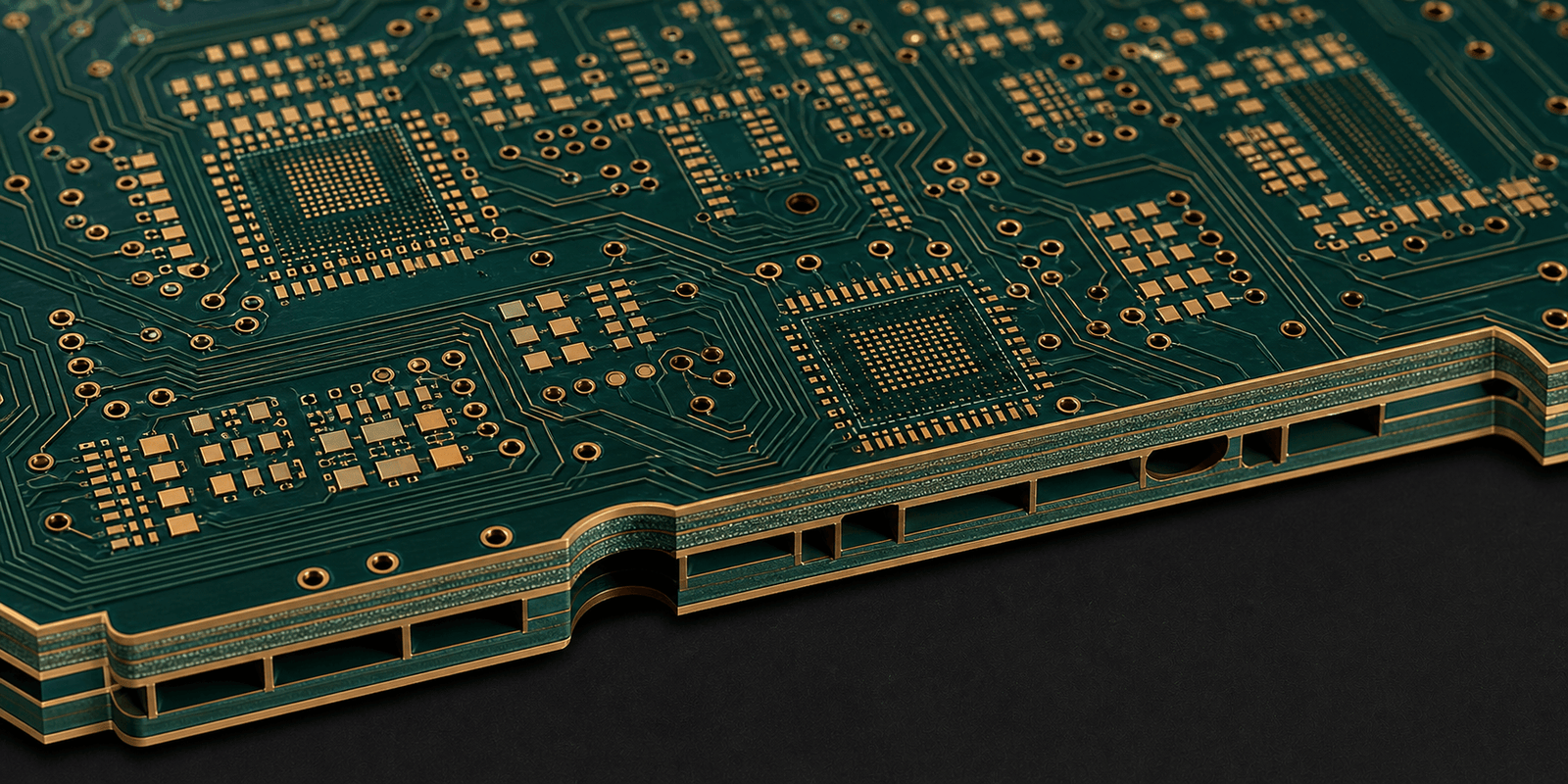
Multilayer Stack-Up Design
Layer stack-up defines the physical construction of the board: the number of copper layers, their sequence, the dielectric materials between them, and the finished board thickness. Stack-up decisions made before layout begins determine trace impedance control capability, power delivery performance, EMC behaviour and fabrication cost. A provider with multilayer experience will define the stack-up in consultation with the intended fabrication house – not retrospectively. For mixed-signal and RF designs, layer assignments for reference planes, power planes and signal routing layers are primary EMC design controls. IPC-2221B, the generic standard for printed board design, provides the foundational layer assignment and geometry guidelines that govern professional multilayer design practice.
Signal Integrity and High-Speed Design
As digital interface speeds increase, PCB layout transitions from a connectivity task to a signal integrity engineering problem. USB 3.0, PCIe, Gigabit Ethernet, MIPI CSI/DSI, LPDDR memory and high-speed ADC interfaces all impose controlled-impedance requirements, matched-length differential pair routing, and return path continuity rules that directly affect functional yield. A circuit board design service that handles high-speed work applies these rules systematically: impedance-controlled trace widths derived from the stack-up, differential pair tuning within tolerance, reference plane continuity under critical signals, and via stitching to maintain ground reference integrity. Designs that ignore these requirements may appear to work at prototype stage but fail at production where board-to-board variation is larger.
EMC-Aware Layout
Electromagnetic compatibility is engineered throughout the layout process, not applied as a post-design filter. EMC-aware PCB design applies continuous reference planes to minimise return current loop area, routes switching power signals away from analogue inputs, applies common-mode filtering at board entry and exit points, and places decoupling capacitors with minimum loop inductance. For products sold in Australia, the ACMA EMC framework and the Regulatory Compliance Mark (RCM) regime define the electromagnetic emission and immunity requirements that finished products must meet. Designs that address EMC at the layout stage pass pre-compliance testing at significantly higher rates and require fewer costly redesign cycles before certification.
Design for Manufacture Review
DFM review is the systematic evaluation of the completed PCB layout against the process capabilities, tolerances and preferences of the fabrication and assembly house. It covers pad geometries, solder mask clearances, paste stencil aperture ratios, via minimum drill sizes, component-to-edge clearances, assembly process direction and thermal relief requirements for SMD pads on copper planes. A thorough DFM pass – informed by IPC-2221B and the specific fab’s DFM guidelines – is the single most effective risk reduction step before first-article fabrication. It is a standard deliverable in a professional circuit board design service, not an optional extra. Zeus Design’s electronics design service includes DFM review as a standard part of every PCB design engagement.
Production Output Package
The production output package is the tangible deliverable that enables fabrication and assembly. A complete package includes Gerber RS-274X or Gerber X2 files for every copper and non-copper layer, an NC drill file, a bill of materials with manufacturer part numbers and approved alternates, a pick-and-place centroid file, assembly drawings with component polarity and orientation callouts, and an IPC-356 netlist for assembled board electrical test. Incomplete output packages are a common source of fabrication delays and unexpected costs. A professional service delivers a verified, complete package that a fabrication house and contract manufacturer can act on without a back-and-forth clarification cycle.
When Your Project Needs This Service
Not every PCB project needs a full external circuit board design service. Simple two-layer designs with relaxed timing requirements and standard through-hole or large-pitch SMD components can often be managed by a capable electronics engineer without specialist PCB layout support. The need for a professional circuit board design service increases with four factors: layer count, signal speed, component density and compliance requirements.
Projects that reliably justify a specialist engagement include: four-layer and above designs with controlled-impedance requirements; designs integrating wireless RF modules where antenna placement and ground plane geometry affect emissions and receiver sensitivity; high-density interconnect (HDI) layouts with microvias and fine-pitch BGA components; products targeting medical device, defence or automotive end markets where design documentation and traceability requirements are formal; and designs where first-article failure cost is high – either in prototype turnaround time or in the risk of a costly re-spin delaying a production launch.
For teams approaching their first hardware product, an integrated service that combines circuit board design with rapid electronics prototyping reduces the handoff friction between design completion and first physical validation. A design partner who also builds and tests the first prototypes has direct incentive to design for assembly and test access, and brings functional test findings directly back into the layout rather than relying on written defect reports.
Technical and Commercial Risks to Manage
Understanding the most common failure modes in circuit board design engagements helps product teams ask the right questions and structure their engagement to avoid them.
Schematic-to-Layout Synchronisation Errors
In manually managed workflows, changes to the schematic after layout has begun can fail to propagate correctly to the PCB, resulting in connectivity errors that only appear during board bring-up. Modern EDA platforms with tight schematic-PCB synchronisation reduce this risk, but it requires that the design team works within the platform’s synchronisation workflow – not around it with manual net list exports. Ask prospective providers what EDA toolchain they use and how they manage schematic revisions during layout.
Stack-Up Frozen Too Late
Stack-up decisions made after significant routing work has been completed create expensive rework. Impedance targets depend on trace width and layer dielectric properties; if the stack-up changes, impedance-controlled traces must be rerouted. A professional circuit board design service defines the stack-up in coordination with the fabrication house before layout begins, confirming the dielectric materials and layer thicknesses that the fab will use in production.
DFM Issues Discovered Post-Fabrication
DFM issues caught by the assembly house after boards arrive for population result in delays, additional charges and sometimes complete first-article scraps. The most common issues are insufficient solder mask clearances, paste aperture ratios outside the stencil printer’s capability range, and component placements that prevent the board from being processed in a single reflow pass. A formal DFM review before Gerber release eliminates these as surprises.
Compliance Planning Deferred
Teams that treat EMC and regulatory compliance as a post-design test step rather than a design input consistently spend more on certification. Pre-compliance EMC planning at the layout stage – selecting filter component locations, planning board entry and exit points, and designing PCB shielding provisions – is far cheaper than a schematic and layout redesign triggered by a failed emissions test. For Australian products requiring RCM, engagement with a compliance-aware design service early in the project timeline is the most cost-effective approach.
Zeus Design: Circuit Board Design for Australian Hardware Teams
Zeus Design provides a full-scope circuit board design service for hardware teams across Australia. The engagement covers the complete process from component selection and schematic capture through multilayer PCB layout, DFM review and production output package. Designs are completed in Altium Designer; clients receive native Altium project files as part of the deliverable package, retaining full design ownership and the ability to continue development in any Altium-licensed environment.
Zeus Design works in Altium Designer across the full design flow: schematic capture with formal review, multilayer stack-up definition in consultation with the intended fabrication house, EMC-aware component placement and routing, signal integrity analysis for high-speed interfaces, and a comprehensive DFM review before production output. The production output package covers Gerber files, NC drill, BOM with approved alternates, pick-and-place centroid data, assembly drawings and IPC-356 netlist.
Where a project also requires firmware, the embedded software development team works alongside the PCB design team from the start of the engagement. This parallel structure surfaces hardware-software interface decisions early – pin assignments, peripheral configuration, power sequencing requirements and boot dependencies – before they are frozen in layout. The result is a shorter hardware-software integration phase and fewer prototype iterations caused by late-discovered firmware-hardware conflicts.
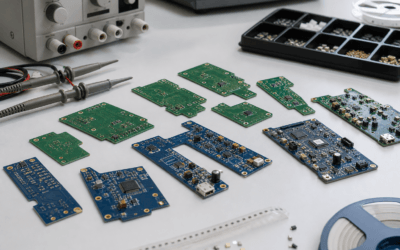
For teams at earlier stages, Zeus Design’s rapid electronics prototyping service provides quick-turn PCB builds, functional testing and iteration support. The same team that designs the board also manages the first prototype build and test, which means DFM and test access considerations are built into the layout from the first revision rather than retrofitted after a difficult first-article assembly.
How This Connects to Related Services
Circuit board design sits at the centre of a hardware product development programme but connects directly to services that precede and follow it. Upstream, electronics design covers the system architecture and circuit design decisions that the PCB layout implements. Downstream, rapid prototyping converts the PCB design into a functional physical board for test and validation. After prototyping, DFM review bridges the gap between a validated prototype layout and a production-stable design that an assembly house can manufacture at yield.
For connected products, PCB design integrates with embedded software development and IoT connectivity work. The circuit board provides the physical substrate for the firmware; decisions about processor selection, memory architecture, peripheral interfaces and wireless module integration are made jointly across electronics and software. Zeus Design’s integrated delivery model – covering electronics design, PCB layout, embedded software and IoT connectivity within the same team – reduces the coordination overhead that arises when these disciplines are split across separate vendors.
The published blog posts on how the PCB process works in 2026 and PCB design services in Australia cover the technical process and service evaluation criteria in further depth for teams researching the full landscape.
FAQs
What does a circuit board design service actually deliver?
A professional circuit board design service delivers a complete set of production-ready design outputs: schematic, multilayer PCB layout in a professional EDA tool, DFM review documentation, and a full production output package covering Gerber files, NC drill, BOM with manufacturer part numbers, pick-and-place centroid data and assembly drawings. The client retains full IP ownership of all deliverables. Zeus Design also provides native Altium Designer project files so clients are not locked into a vendor-specific format.
How long does a circuit board design service engagement take?
Timeline depends on design complexity, layer count and the completeness of the electrical specification at engagement start. A straightforward 4-layer IoT device design with a well-defined schematic input can complete in two to four weeks. A complex 10-plus-layer high-speed design with BGA components, controlled impedance and formal EMC planning typically takes six to twelve weeks including DFM review and production output. Timeline estimates improve substantially once the full project scope is defined in a brief.
What is the difference between circuit board design and PCB layout?
PCB layout is the physical routing and component placement step within a broader circuit board design service. A complete service also includes component selection review, schematic capture and review, stack-up definition, signal integrity analysis, EMC planning, DFM review and production output generation. Teams that engage a service for layout only – providing a completed schematic – receive a narrower scope; teams that engage for the full circuit board design process receive an end-to-end engineering service.
Why use an Australian circuit board design service rather than offshore?
Australian hardware teams benefit from local circuit board design services through regulatory familiarity, time-zone-aligned collaboration and direct technical access. Australian designers are familiar with the RCM compliance framework, AS/NZS standards and local fabrication and assembly house capabilities. For complex projects, the ability to review layout decisions in real time – without a 12-hour asynchronous delay – materially reduces design cycle time. IP jurisdiction is also cleaner with a local engagement, which matters for products entering regulated or defence-adjacent markets.
When should I involve the circuit board design service in the project?
The earlier the better. Involving a circuit board design service at the system architecture stage – before component selection is finalised – allows the PCB design team to flag layout constraints that affect component choice, package selection and interface decisions. Stack-up, layer count and EMC compliance planning decisions made at the start of the project are significantly cheaper than changes made after layout has begun. For teams at concept stage, a design review or feasibility discussion with Zeus Design can prevent the most expensive early mistakes.
Does Zeus Design work on small production volumes and hardware startups?
Yes. Zeus Design works with hardware startups from proof-of-concept through to production-ready design. The circuit board design service scales from single-layer proof-of-concept boards through complex multilayer production designs. For early-stage projects, the integrated rapid prototyping capability means the same team that designs the board can also manage the first prototype build and functional test, providing direct feedback into the layout before the design is released for volume production.
What EDA tools does Zeus Design use for circuit board design?
Zeus Design works in Altium Designer for schematic capture, PCB layout, simulation and production output generation. Altium Designer is the industry’s leading professional PCB design platform for production-intent designs. Clients receive native Altium project files as part of the deliverable package, giving them full design ownership and the ability to continue development internally or with any other Altium-licensed provider. Altium Designer maintains a live, bidirectional link between schematic and layout, which eliminates the class of synchronisation errors that arise in less integrated workflows.
Conclusion
A professional circuit board design service is a structured engineering engagement covering component selection, schematic capture, multilayer PCB layout, EMC-aware routing, DFM review and complete production output – not a commodity layout task. For Australian hardware teams, the combination of local regulatory familiarity, time-zone-aligned collaboration and integrated firmware capability makes a local design partner the lower-risk choice on complex or compliance-sensitive projects.
The highest-return investments in any circuit board design engagement are stack-up planning before layout begins and DFM review before Gerber release. Both are significantly cheaper than the redesign cycles they prevent. Teams that treat compliance planning as a design input rather than a post-prototype test also consistently reach certification with fewer redesign iterations.
Zeus Design provides circuit board design services for hardware teams across Australia, from component selection and schematic through production-ready Gerber output, with optional integrated rapid prototyping and embedded software development for teams that need the full development pipeline in one engagement. Contact Zeus Design to discuss your project scope and timeline.
")


0 Comments