
Professional PCB design services cover the full journey from electrical schematic to production-ready Gerber files – including multilayer stack-up, EMC-aware routing, design for manufacture (DFM) review and compliance planning. For hardware startups, product companies and engineering teams across Australia, choosing the right PCB design service is one of the most consequential early decisions in a product development programme. This guide explains what a complete engagement covers, how to evaluate providers, where local and offshore services differ, and how Zeus Design approaches circuit board design for Australian teams.
TL;DR
- PCB design services cover schematic capture, multilayer layout, DFM review, EMC-aware routing and Gerber output – not just physical placement.
- Evaluate providers on EDA toolchain, layer capability, DFM process, signal integrity experience and past work in your industry vertical.
- Australian PCB design services offer regulatory familiarity (RCM), time-zone alignment and direct technical access that offshore providers often cannot match on complex projects.
- DFM review is the most undervalued deliverable – it prevents yield loss before the first board is fabricated.
- Hardware startups gain the most from an integrated service that combines PCB design with electronics design and firmware development.
- Zeus Design works in Altium Designer and delivers full production output packages with native project files retained by the client.
- Pre-compliance EMC planning at the layout stage is far cheaper than a post-certification redesign.
Who Uses PCB Design Services – and Why
PCB design services are used by a wide range of organisations, but the need is most acute in three situations: when a team lacks in-house PCB layout capability, when the design complexity exceeds what the in-house team can confidently handle (dense BGAs, high-speed interfaces, RF), or when turnaround speed is critical and additional design capacity is needed.
In the Australian market, the typical clients for professional PCB design services include hardware startups bringing a first product to market, established product companies developing next-generation hardware, and engineering consultancies that need design capacity for client projects. Defence, medical devices, industrial automation and IoT-connected products are the verticals where design quality is most tightly linked to commercial and regulatory outcomes.
Understanding which category you fall into helps frame what you should be asking of a prospective design partner – and which service attributes matter most to your specific situation.
What PCB Design Services Include
A professional PCB design engagement covers considerably more than routing copper on a board. The following components make up a complete service offering.
Schematic Capture and Review
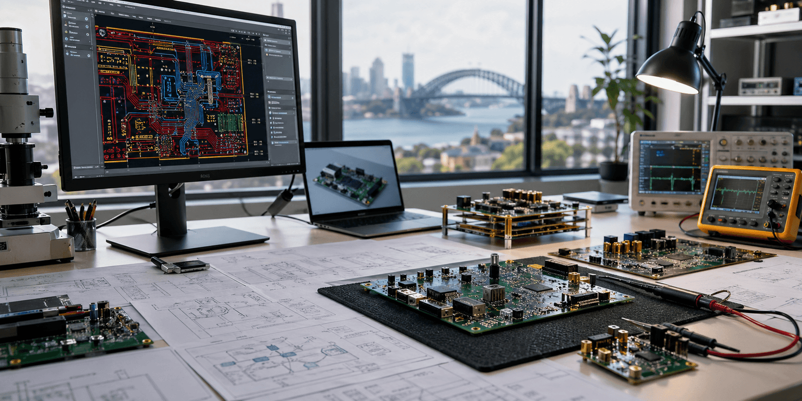
Schematic capture translates the electrical design intent into a structured, hierarchical drawing that defines all components, their connections and functional boundaries. A complete service includes a formal schematic review – checking for errors in net connectivity, missing decoupling, incorrect component values and interface compatibility issues – before layout begins. Errors caught at the schematic stage cost a fraction of what they cost to fix after routing is complete. The Altium Designer schematic environment provides full forward-annotation to the PCB layout, eliminating a class of manual synchronisation errors that affect less integrated toolchains.
Multilayer Layout and Stack-Up Design
Layer stack-up defines the physical construction of the board: copper layers, dielectric materials, and thicknesses. Stack-up decisions made early in a project control impedance, signal integrity, power delivery performance and fabrication cost. A provider with multilayer experience will define the stack-up in consultation with the intended fabrication house – not as an afterthought. For mixed-signal and RF designs, layer assignments for ground planes, power planes and signal layers are a primary EMC control mechanism, not a secondary concern.
EMC-Aware Routing
Electromagnetic compatibility (EMC) is not an afterthought applied at the end of layout – it is an engineering discipline that shapes decisions throughout the design process. EMC-aware PCB design services apply continuous ground planes to minimise return current loops, control trace impedance for high-frequency signals, route differential pairs with matched length and spacing, apply filtering at board entry and exit points, and separate switching and sensitive analogue circuits. Designs that address EMC at the layout stage pass pre-compliance testing at significantly higher rates than those that treat it as a post-design problem. The AS/NZS CISPR 32 standard governs electromagnetic disturbance limits for multimedia equipment in Australia and is directly relevant to the EMC design requirements of many consumer and commercial electronics products.
Design for Manufacture (DFM)
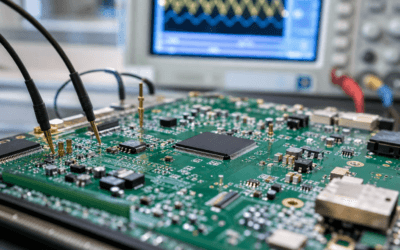
DFM review is the systematic evaluation of the completed PCB layout against the process capabilities and tolerances of the fabrication and assembly house. It covers pad geometries, solder mask clearances, paste stencil aperture ratios, via specifications, component-to-edge clearances and assembly process constraints. A thorough DFM pass – informed by IPC-2221B and the specific fab’s DFM guidelines – is the single most effective way to reduce the probability of a costly first-article failure. It is a standard deliverable in a professional PCB design service, not an optional extra.
Gerber Generation and Production Output Package
The production output package is the tangible deliverable that enables fabrication and assembly. It includes Gerber RS-274X or Gerber X2 files for every copper and non-copper layer, an NC drill file, a bill of materials (BOM) with manufacturer part numbers, a pick-and-place centroid file, assembly drawings and an IPC-356 netlist. Incomplete output packages are a common source of delays and unexpected charges from fabrication houses – a professional PCB design service delivers a verified, complete package.
How to Evaluate PCB Design Services
Not all PCB design services are equivalent. The following criteria provide a structured framework for assessing a prospective provider.
EDA Toolchain and Capability
The EDA (electronic design automation) software used by the design team affects schematic quality, library management discipline, simulation capability and the integrity of the production output. Altium Designer is the industry’s leading professional PCB design platform for complex, production-intent designs; it provides tightly integrated schematic, layout, simulation and output workflows. Providers working in professional toolchains are less likely to introduce integration errors between schematic and layout, and produce output packages that are recognised by Australian and international fabrication houses without format conversion.
Layer Count Experience
Ask prospective providers about their experience with designs of comparable complexity to yours. A provider comfortable with two-layer power supplies may not have the signal integrity discipline required for a six-layer design with a GigE interface and DDR memory. Request examples (redacted if necessary) of multilayer work in your complexity range, and ask specifically about controlled impedance, differential pair routing and high-speed design review processes.
DFM Process and Fabrication House Relationships
A design partner with established relationships with fabrication houses – particularly Australian-accessible fabs – will design to those houses’ actual process capabilities rather than a generic standard. Ask whether DFM review is included as standard, whether the output package is verified against the fab’s file specification before delivery, and what happens when a DFM issue is identified after output generation. The answer to this last question is telling: a provider with a robust DFM process resolves issues before output; one without one discovers them after.
Compliance and Regulatory Experience
Products sold in Australia require RCM (Regulatory Compliance Mark) authorisation, which encompasses EMC and electrical safety standards administered by the Electrical Regulatory Authorities Council (ERAC). A PCB design service with compliance experience will design with RCM in mind from the outset – not as a post-design problem. Ask whether the provider has supported products through RCM or CE/FCC certification, and whether they offer pre-compliance planning as part of the design engagement.
Integration with Electronics and Firmware Development
PCB layout does not exist in isolation. When PCB design, circuit design and firmware development are performed by separate teams with limited communication, the result is typically a higher number of hardware revisions and a longer time to a working system. Providers that offer integrated electronics design and firmware development alongside PCB layout – or that have structured processes for handoff between disciplines – materially reduce the risk of design iterations driven by misaligned assumptions between hardware and software teams.
Local vs Offshore PCB Design Services for Australian Teams
Australian companies sourcing PCB design services face a genuine choice between local providers and offshore alternatives in India, Eastern Europe and South-East Asia. The decision is not straightforward, and the right answer depends on project complexity, regulatory requirements and how much the team can absorb in communication overhead.
The Case for Local Australian PCB Design Services
Australian PCB design services provide time-zone-aligned communication – which, on a complex project with frequent questions and decisions, is worth more than it appears in a rate comparison. Local providers understand the RCM regulatory environment, are familiar with Australian and accessible Asia-Pacific contract manufacturers, and can participate in face-to-face or video design reviews during business hours. For products with compliance requirements, medical device classifications, or safety-critical applications, the ability to have direct, real-time technical conversations throughout the design process significantly reduces misalignment risk.
Local providers also carry accountability that is practically enforceable under Australian law – a factor that matters when a project involves significant IP or commercial consequence.
Where Offshore Services Can Work
For straightforward designs – a two- or four-layer board with well-understood interfaces, no compliance complexity and a clear, complete specification – offshore PCB design services can deliver at lower headline cost, particularly for teams with experience managing offshore technical engagements and the capacity to perform thorough review of delivered work. The risk increases proportionally with design complexity, interface speed, component density and regulatory requirements. Projects that involve multiple rounds of schematic review, DFM iteration and compliance planning typically see the rate differential erode when total engagement cost – including revision cycles and communication overhead – is accounted for.
A Practical Decision Framework
Consider local Australian PCB design services when: the design involves high-speed interfaces, RF, multilayer complexity or compliance requirements; the team cannot afford a lengthy revision cycle; the product is subject to RCM authorisation; or the design must integrate tightly with in-house firmware development. Consider offshore services when: the design is a well-defined, low-complexity board with a complete and stable specification; the team has the engineering capacity to perform a thorough review of deliverables; and schedule compression is not critical.
Zeus Design’s PCB Design Service
Zeus Design’s circuit board design service covers the full PCB design workflow – from schematic capture through multilayer layout, EMC-aware routing, DFM review and production output generation – for hardware startups and product companies across Australia.
All designs are completed in Altium Designer, with full schematic-to-layout connectivity, integrated simulation capability and verified Gerber X2 output. The engagement process follows a structured sequence:
- Requirements and specification review: Functional requirements, interface specifications, target layer count, mechanical envelope, regulatory targets and production volume are agreed before design work begins.
- Schematic capture and formal review: Circuit design is completed and reviewed with the client against the functional specification. Layout does not begin until schematic review sign-off is received.
- Stack-up definition: Layer stack-up is selected in consultation with the intended fabrication house to match achievable impedance targets, dielectric properties and cost profile.
- Component placement and routing: Placement is optimised for signal integrity, thermal management, assembly process compatibility and mechanical constraints. Routing follows with DRC validation at each stage and signal integrity review for critical nets.
- DFM review: Completed layout is reviewed against the fabrication and assembly house’s DFM checklist and relevant IPC standards. All identified issues are resolved before output generation.
- Production output package: Gerber X2, NC drill, BOM, pick-and-place centroid, assembly drawings and IPC-356 netlist are generated, verified and delivered alongside the full native Altium project.
Clients retain the native Altium project files – not just the output package – so the design is accessible for future revisions without toolchain dependency on Zeus Design.
Zeus Design’s PCB design capability is strongest on projects where design complexity, compliance requirements or integration with firmware development makes the local, integrated model demonstrably more efficient than a fragmented, offshore engagement. The team has experience across IoT products, industrial electronics, medical-adjacent devices and consumer hardware at various stages of development – from first prototype through to production-ready design.
Related Services
PCB design integrates directly with several adjacent services that affect the overall success of a hardware product development programme.
Electronics Design
Circuit design and PCB layout are most effective when performed as an integrated engagement. Zeus Design’s electronics design service covers analog and digital circuit design, component selection, power architecture, signal chain design and compliance planning – all of which directly inform and are informed by the PCB layout process. Teams that separate these disciplines typically see more design iterations and longer time to a working prototype.
Rapid Electronics and PCB Prototyping
Once PCB design files are complete, moving quickly to a working prototype is the most effective way to validate functional and EMC performance before committing to production quantities. Zeus Design’s rapid prototyping service supports quick-turn prototype builds – from bare board procurement through to assembled and tested functional units – that allow issues to be identified and resolved at low cost and calendar impact.
Embedded Firmware Development
Hardware and firmware co-development reduces the risk of integration failures that are only discovered when firmware runs on real hardware. Starting firmware development against a hardware simulation model or early prototype, with the PCB design team accessible for clarification, compresses the integration phase and reduces the probability of a hardware revision driven by firmware assumptions about peripheral behaviour, power sequencing or interrupt latency.
FAQs
What do PCB design services typically cost in Australia?
Cost varies considerably with design complexity, layer count and turnaround requirements. Simple two- to four-layer designs for straightforward products may be quoted from a few thousand dollars. Complex multilayer designs with high-speed interfaces, controlled impedance, RF or dense BGAs – and full DFM review – will carry higher fees that reflect the engineering time involved. Rate comparisons with offshore providers should account for total engagement cost, including revision cycles, not just the headline design fee.
How long does a PCB design services engagement take?
A simple two-layer design with fewer than 50 components typically takes 1-2 weeks. A complex multilayer design with high-speed interfaces, a comprehensive schematic review and full DFM pass typically takes 4-8 weeks. Timeline is also affected by how promptly the client provides schematic review feedback, component approvals and specification clarifications – prompt responses are the most effective way a client can keep a design project on schedule.
What should I provide to a PCB design service at the start of an engagement?
At minimum: a functional specification covering electrical interfaces, power requirements and operating conditions; any mechanical constraints (board size, connector locations, mounting points); target production volume; regulatory requirements (RCM, CE, FCC); and any preferred or mandatory components. A schematic – even a partial or conceptual one – is highly valuable. The more complete and stable the specification at engagement start, the lower the probability of costly mid-design changes.
Can PCB design services help with compliance and RCM certification?
Yes – and compliance planning at the PCB design stage is far more cost-effective than a post-failure redesign. EMC-aware layout practices (ground plane continuity, return current path control, filtering, shielding) are the primary hardware mechanism for meeting CISPR radiated and conducted emissions limits. A PCB design service with RCM experience will incorporate these practices by default, and can advise on pre-compliance testing strategy before formal submission.
Do I own the PCB design files after the engagement?
Ownership of design files should be clarified in the engagement agreement before work begins. Zeus Design delivers the full native Altium project to the client alongside the production output package, ensuring the client retains full access to and ownership of the design for future revisions, manufacturing changes and product development without dependency on the design service provider’s toolchain.
How do I know if my design needs controlled impedance?
Controlled impedance is required when trace propagation delay and reflections materially affect signal performance – generally at data rates above 100 Mbps, for RF signal paths, and for any differential pair interface (USB, HDMI, PCIe, GigE, DDR). If your design includes any of these interfaces, controlled impedance traces and a stack-up specified to achieve target impedance at the fabrication house are not optional. Your PCB design partner should be identifying this requirement, not leaving it to you to ask about.
What is the difference between a PCB design service and a PCB layout service?
A PCB layout service typically covers only the physical placement and routing phase, assuming a schematic is provided. A PCB design service covers the full engineering process: schematic capture, component selection, stack-up definition, placement, routing, DFM review and production output generation. For most hardware product development projects – particularly where compliance, signal integrity or first-spin success matters – a full design service is the appropriate engagement, not layout-only.
Ready to Discuss Your PCB Design Project?
Zeus Design provides pcb design services to hardware startups and product companies across Australia – from first-prototype boards through to production-ready multilayer designs with EMC planning, DFM review and complete Gerber output packages. If you are evaluating design partners or have a project ready to scope, the best starting point is a direct conversation about your requirements.
")


0 Comments