
Circuit design services cover the electrical engineering work that happens before a single trace is routed on a PCB – schematic capture, component selection, simulation and the handover package that makes layout possible. This guide is written for engineers and product managers evaluating a development partner who need to understand what circuit design actually involves, where it differs from PCB layout, and what a properly executed schematic stage delivers before production.
TL;DR
- Circuit design is the discipline that defines what a product does electrically – PCB layout defines how that design behaves physically. They are sequential but distinct engineering activities.
- Good circuit design includes component selection for long-term supply availability, not just electrical fit on a datasheet.
- Simulation – SPICE for analog sections, timing analysis for digital buses – catches design errors while they are still cheap to fix.
- A clean schematic-to-layout handover package includes a reviewed schematic, net classes, a draft BOM and design intent notes for the layout engineer.
- DFM thinking starts at the schematic stage – footprint selection, package choice and power architecture all affect manufacturability before layout begins.
- Zeus Design provides analog and digital circuit design as part of its electronics design service, with a structured handover into circuit board design and PCB layout.
Why Circuit Design Is a Distinct Discipline From PCB Layout
It is easy to think of hardware development as one continuous task: design the circuit, lay out the board, build it. In practice, circuit design and PCB layout require different skills, different tools and different ways of thinking about the same product. Circuit design is concerned with electrical behaviour in the abstract – what voltage appears where, how a signal is generated and conditioned, what happens to the circuit at temperature extremes or under load. Layout is concerned with the physical realisation of that behaviour on a board with finite space, copper and manufacturing tolerances.
Product teams who blur this distinction often under-scope circuit design services, assuming the schematic is a quick step before the “real work” of layout begins. That assumption causes problems downstream. A schematic with an under-specified power architecture, an ambiguous net topology or a component chosen purely on electrical performance without checking footprint or availability creates rework that surfaces during layout, prototyping or – worse – after a production run has started.
Circuit design services exist to do this stage properly: define the architecture, select components against multiple criteria, simulate critical sections, and produce a schematic that a layout engineer can implement without having to guess at design intent. Zeus Design’s electronics design service treats circuit design as a dedicated phase with its own review gate before any layout work starts.
What Circuit Design Services Cover
Requirements Translation and Architecture Definition
Before a schematic exists, circuit design starts with translating product requirements into an electrical architecture: power budget and supply rails, processor or microcontroller selection, sensor and interface requirements, and the high-level block diagram that shows how subsystems connect. This stage sets the ceiling on what the product can do – a power architecture that cannot supply peak current, or a microcontroller without enough peripherals, will constrain every decision that follows.
Architecture decisions also set the cost baseline. Selecting a processor with integrated peripherals versus discrete components, choosing a linear regulator versus a switching supply, or deciding whether a function needs a dedicated IC or can be handled in firmware all have direct bill-of-materials and development time consequences that are far cheaper to model at this stage than to revisit later.
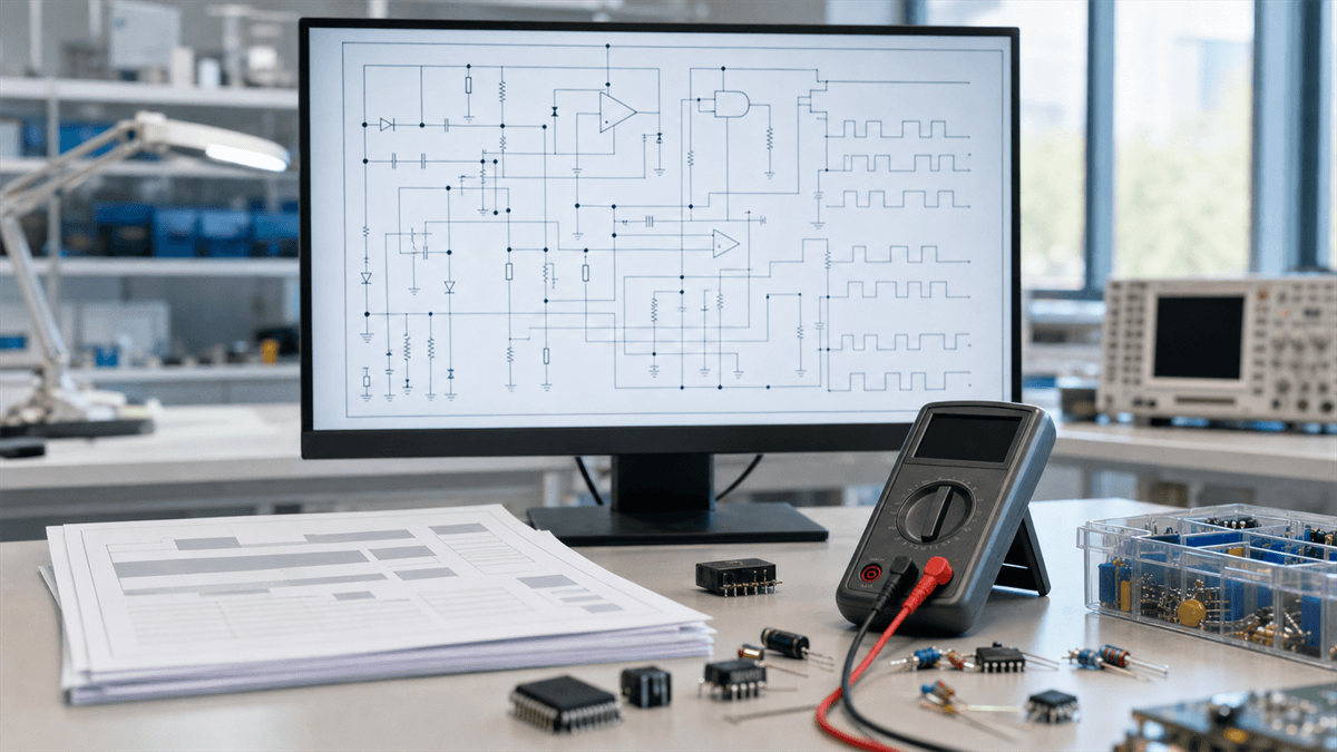
Schematic Capture
Schematic capture is the process of drawing the circuit in a design tool, defining nets, assigning component footprints and documenting design intent. A professionally captured schematic is more than an electrically correct drawing – it is structured for review and for layout. That means logical sheet organisation by function, consistent net naming, clear power rail labelling, and notes that explain non-obvious design choices (why a particular decoupling value was chosen, why a net needs to be kept short, which signals are timing-critical).
Schematic capture also includes setting up the component library correctly – verified footprints, accurate pin mapping and confirmed package data. Library errors are one of the most common sources of late-stage rework: a footprint mismatch discovered after boards are fabricated is far more expensive than catching it during schematic review. Most professional circuit design services use a managed component library workflow inside tools such as Altium Designer, where each part’s symbol, footprint and supplier data are verified once and reused across projects.
Component Selection
Component selection in circuit design services has to satisfy several criteria simultaneously, not just electrical fit:
- Electrical performance – voltage, current, frequency and tolerance specifications that meet the circuit’s operating requirements with adequate margin, not just typical datasheet values.
- Thermal behaviour – package thermal resistance and expected power dissipation checked against the product’s enclosure and ambient operating range.
- Supply chain resilience – lead time, stocked quantities, and the existence of qualified second-source alternates. A component with a single source and a long lead time is a production risk hiding in a schematic.
- Manufacturability – package type and pitch need to match what the target contract manufacturer can reliably place and solder at the intended production volume.
- Lifecycle status – avoiding parts already flagged for end-of-life, which forces a redesign mid-production.
This is also where cost optimisation happens most effectively. Component choices made during circuit design – rather than substituted later under time pressure – are far more likely to balance performance against unit cost correctly. Zeus Design’s cost optimisation capability is applied during this stage of an engagement, not bolted on afterward.
Analog Circuit Design
Analog sections – power supplies, sensor front-ends, amplification stages, analog filtering, RF circuits – typically demand the most engineering judgement in a circuit design engagement. Analog behaviour does not fail cleanly; it degrades. A poorly designed sensor front-end does not stop working, it produces noisy or drifting readings that are difficult to diagnose without test equipment and a strong grasp of the underlying physics.
Good analog circuit design accounts for component tolerance stack-up, temperature coefficients, supply noise rejection and the real operating environment the product will see – not just bench conditions. SPICE simulation is the standard tool for validating analog behaviour before a board exists: it allows a designer to sweep component tolerances, temperature and supply variation to confirm a circuit performs across its full expected range rather than only at nominal values. Texas Instruments’ simulation resources document how vendor-supported SPICE models are used to validate analog reference designs before physical prototyping.
Digital Circuit Design
Digital circuit design covers processor and memory architecture, bus interfaces, clock distribution, digital I/O and the interconnection of digital peripherals such as sensors, displays and communication modules. While digital logic is more deterministic than analog behaviour, digital circuit design still requires careful attention to timing margins, bus loading, decoupling strategy and signal-level compatibility between devices operating at different voltage rails.
Mixed-signal products – the majority of connected devices – require digital and analog circuit design to be coordinated rather than treated as separate problems. A digital switching regulator placed without consideration for an adjacent analog sensor front-end will inject noise that no amount of firmware filtering can fully remove. This is why circuit design services that handle both disciplines under one team, as Zeus Design does through its electronics design capability, tend to produce cleaner outcomes than splitting analog and digital work across separate vendors.
Simulation and Design Verification
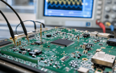
Simulation is where a circuit design is tested before it costs money to build. Depending on the circuit, this can include SPICE simulation of analog stages, timing analysis of digital buses and clock domains, thermal modelling of power dissipation, and worst-case analysis across component tolerance and supply voltage ranges. The goal is to find the conditions under which a design might fail before a prototype board reveals it the hard way.
Worst-case circuit analysis – checking performance at the combination of minimum and maximum component tolerances, supply voltage extremes and temperature limits – is standard practice for circuits with tight margins or safety implications. NASA’s electronic parts and circuit standards document worst-case analysis methodology that, while developed for aerospace reliability requirements, reflects the same engineering discipline applied at a proportionate level in commercial circuit design.
Schematic Review and Handover to Layout
Before a schematic moves to layout, a structured review catches the errors that are cheapest to fix at this stage: missing decoupling, ambiguous net assignments, inconsistent voltage labelling, and footprint mismatches between the schematic symbol and the physical part. This review is a distinct checkpoint, ideally performed by an engineer who did not draw the original schematic, to catch assumptions the original designer may not notice.
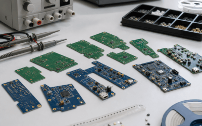
The handover package from circuit design to layout should include more than the schematic file itself. A complete handover typically includes the reviewed schematic, a net class definition (which nets are high-speed, which need controlled impedance, which carry sensitive analog signals), a draft bill of materials with approved part numbers, and design intent notes that explain constraints the layout engineer needs to preserve. Zeus Design’s circuit board design and PCB layout service receives this handover package directly from the circuit design team, which removes the interpretation gap that occurs when schematic and layout are split across separate vendors.
When a Project Needs Dedicated Circuit Design Services
Some projects can move from a rough concept straight into layout with an experienced generalist. Others need a dedicated circuit design phase with its own budget and timeline. Indicators that a project needs dedicated circuit design services include:
- Mixed-signal complexity – any product combining sensitive analog measurement with digital processing or RF circuitry.
- Novel architecture – a first-of-its-kind product where the electrical architecture has not been validated in a previous design.
- Tight power budgets – battery-powered or energy-harvesting products where every milliwatt of quiescent current matters.
- Regulatory or safety-critical circuits – isolation, protection and fault-tolerance requirements that need formal analysis, not rule-of-thumb design.
- Component obsolescence redesign – replacing an end-of-life part requires re-validating the surrounding circuit, not just dropping in a substitute.
If a project sits in one or more of these categories, treating circuit design as a brief precursor to layout – rather than a properly scoped engineering phase – is where avoidable risk gets introduced.
Technical and Commercial Risks to Manage
Component Selection Without Supply Chain Diligence
A component selected purely for electrical performance, without checking stock levels, lead time and second-source availability, can become a production blocker months later. This risk has grown more acute as semiconductor lead times have remained volatile across multiple categories – diligence on sourcing during circuit design avoids discovering a 40-week lead time after tooling is committed.
Insufficient Simulation Coverage
Skipping simulation to save time on a tight schedule is a common but costly shortcut. Analog circuits in particular can appear to work on a single prototype board while failing intermittently across a production run once component tolerance and temperature variation are accounted for. The cost of catching this in simulation is a few hours of engineering time; the cost of catching it in the field is a product recall or warranty claim.
Incomplete Handover to Layout
A schematic handed to a layout engineer without net class definitions, design intent notes or a reviewed BOM forces the layout engineer to make assumptions. Those assumptions are sometimes wrong, and the resulting rework cycle costs more time than a proper handover package would have taken to prepare.
Treating DFM as a Layout-Only Concern
Design for manufacture is often discussed only in the context of PCB layout, but several DFM-relevant decisions are made during circuit design: package selection, pin count, and whether a function is implemented in a single integrated component or several discrete ones. Package and footprint choices are typically benchmarked against standards such as IPC-7351 for land pattern geometry, which exists precisely because component-level decisions made before layout determine whether a board can be assembled reliably. A circuit designer who ignores manufacturability hands the layout and assembly stages problems that originated earlier in the process.
Zeus Design’s Circuit Design Service
Zeus Design provides analog and digital circuit design as a core engineering capability, covering requirements translation, schematic capture, component selection, simulation and the structured handover into PCB layout. The team works across both analog and digital domains, which matters for the mixed-signal products that make up most connected hardware today.
A typical circuit design engagement with Zeus Design produces:
- A reviewed, fully annotated schematic with net classes and design intent notes.
- A draft bill of materials with approved manufacturer part numbers and qualified alternates.
- Simulation results for critical analog and timing-sensitive digital sections.
- A documented power budget and thermal estimate for the design.
- A schematic-to-layout handover package ready for the PCB layout team.
Because circuit design and circuit board design sit inside the same team, the handover into PCB layout happens without the interpretation gap that appears when schematic and layout work are split across separate vendors. The engineers who defined the circuit’s intended behaviour are available throughout layout to clarify design intent and approve any deviations the physical implementation requires.
How Circuit Design Connects to Related Services
Circuit design rarely stands alone in a hardware development project. Understanding how it connects to the stages before and after helps product teams plan engagements with realistic scope and timeline.
Downstream: PCB Layout and Production Handover
A completed and reviewed schematic feeds directly into PCB layout, where component placement, routing and stack-up decisions implement the circuit physically. Zeus Design’s earlier guide on PCB layout services covers what happens after schematic handover, including stack-up selection, signal integrity and DFM review.
Parallel: Embedded Firmware Development
Firmware development can start as soon as the circuit architecture – particularly the processor, memory map and peripheral configuration – is settled, well before layout is complete. Zeus Design’s embedded software development service works from the circuit design team’s architecture decisions to begin driver and bring-up code in parallel with hardware development.
Upstream: Feasibility and Proof of Concept
For genuinely novel products, circuit design is often preceded by a feasibility study or proof-of-concept build that validates the core electrical approach before committing to a full schematic. Zeus Design’s rapid prototyping service supports this early validation work using breadboard or quick-turn prototype builds.
FAQs
What do circuit design services actually include?
Circuit design services cover requirements translation into an electrical architecture, schematic capture, component selection, analog and digital circuit design, simulation, and the handover package that prepares a design for PCB layout. The deliverable is a reviewed schematic and supporting documentation, not a finished board – layout and fabrication are separate, downstream stages.
What is the difference between circuit design and PCB layout?
Circuit design defines what a circuit does electrically – component selection, schematic capture and simulation. PCB layout defines how that design is physically realised – component placement, trace routing, layer stack-up and DFM. Both disciplines are required for a manufacturable product, and Zeus Design’s circuit board design service covers the layout stage that follows circuit design.
Why does circuit design need simulation if a prototype will be built anyway?
Simulation finds problems that a single prototype board often cannot reveal, because one physical sample does not capture the full range of component tolerance, temperature and supply voltage variation a production run will see. Catching a marginal design in simulation costs a few hours of engineering time; catching it after volume production has started costs a recall, a redesign, or both.
How does component selection during circuit design affect production later?
Component selection that only checks electrical performance without considering lead time, stocked availability, second sources and lifecycle status creates production risk that surfaces months after the schematic is finished. A circuit design service that diligences supply chain resilience during component selection – alongside electrical fit – reduces the chance of a forced mid-production redesign.
Can circuit design and firmware development happen at the same time?
Yes, and for connected products it usually should. Once the processor, memory map and peripheral configuration are settled during circuit design, firmware engineers can begin driver development and architecture work without waiting for the schematic to be fully finalised or for PCB layout to complete. Zeus Design coordinates circuit design and embedded software development so both teams work from the same architecture decisions.
What should a schematic handover package include before layout starts?
A complete handover package includes the reviewed schematic, net class definitions identifying high-speed and sensitive analog nets, a draft bill of materials with approved part numbers, and design intent notes covering any non-obvious constraints. Handing over a schematic file alone, without this context, forces the layout engineer to guess at design intent and increases the chance of rework.
Does Zeus Design offer circuit design services on their own, without PCB layout?
Yes. Zeus Design can scope a circuit design engagement on its own – for example, to validate an architecture, review an existing schematic, or support a team that has in-house layout capability but needs analog or digital circuit design expertise. Most engagements, however, benefit from continuity between circuit design and the electronics design service that follows it through to production.
Conclusion
Circuit design services define the electrical foundation that everything downstream – layout, prototyping, firmware, manufacturing – is built on. Schematic capture, component selection, analog and digital circuit design, and simulation are where a product’s performance, reliability and manufacturability are largely determined, well before a PCB exists. Treating this stage as a quick step before the “real work” of layout begins is one of the more avoidable sources of cost and delay in hardware development.
For engineers and product managers evaluating a development partner, the questions worth asking are about process: how component selection accounts for supply chain risk, what simulation coverage looks like for analog and timing-critical sections, and what the handover package to layout actually contains. Those answers tell you more about engagement quality than a quoted hourly rate.
Zeus Design provides analog and digital circuit design as part of an integrated electronics design service, with a structured handover into circuit board design and production. If you have a concept that needs a properly scoped schematic, or an existing design that needs circuit-level review before moving to layout, get in touch to discuss scope.


0 Comments