
Choosing custom PCB Australia design has become a real decision point for product teams, not a default – many founders now weigh a local design house against an offshore design-and-build package before committing budget. This guide is written for hardware startup founders, product managers and engineering leads who need to decide where their board gets designed, who will own intellectual property risk, and how design-for-manufacture (DFM) discipline differs between a local partner and an offshore one. You will come away with a clear framework for making that call rather than a generic pros-and-cons list.
TL;DR
- Custom PCB Australia design through a local house gives you faster iteration cycles, easier IP protection under Australian law, and DFM aligned to local contract manufacturers.
- Offshore design-and-build packages can look cheaper on a quote but often shift cost and risk into rework, IP exposure and longer change-request turnaround.
- IP protection is contractual, not automatic – trade secrets and design files need confidentiality agreements and controlled data-sharing regardless of where the work happens.
- DFM review tied to a specific local contract manufacturer’s process capabilities reduces respins more reliably than generic design rules applied for an unknown offshore factory.
- Time zone alignment and in-person design reviews matter more than most budgets account for, especially during bring-up and first production run.
- Zeus Design delivers custom PCB design and rapid prototyping from an Australian base, with DFM built into the process rather than checked at the end.
- The right answer is often hybrid: local design and DFM, with manufacturing volume sourced wherever it makes commercial sense once the design is locked.
Context: Why This Decision Matters More Than It Used To
A few years ago, “custom PCB Australia” searches were mostly about finding any competent designer. Today the question has sharpened: with offshore design bureaus advertising fast turnaround and low headline pricing, and with global supply chains under renewed pressure, product teams are asking whether local design is worth a price premium – and what they are actually buying when they pay it.
The answer depends heavily on what stage your product is at. A hobbyist board or a single proof-of-concept carries low stakes either way. A funded hardware startup preparing for its first production run, or an industrial business commissioning a board that will sit inside regulated equipment, has materially more to lose from a design partner who is hard to reach, slow to iterate, or loose with design data. This guide focuses on that second group, where the decision has real commercial consequences.
Australia’s own manufacturing strategy has leaned back toward local capability in recent years, with government funding directed at advanced manufacturing and supply chain resilience. That shift is also visible in how product teams brief PCB design work: more requests now explicitly ask for local design, local DFM alignment and a clear data-handling policy, rather than just a price per board.
What “Custom PCB Australia” Actually Covers
Custom PCB design is the process of taking a product’s functional requirements and producing a purpose-built circuit board – schematic capture, multilayer layout, signal integrity and EMC-aware routing, DFM review and a production-ready Gerber package – rather than adapting an off-the-shelf module. For a deeper walkthrough of that process end to end, see Zeus Design’s guide to custom PCB design services for product teams.
The “Australia” qualifier matters because it changes three things: who you can talk to in real time, which regulatory and compliance context the design is built against, and which contract manufacturer’s process the DFM review is actually checking against. Those three factors are where the local-vs-offshore comparison plays out in practice.
Local Design House: What You Are Actually Paying For
Faster, Lower-Friction Iteration
Time zone alignment is easy to underweight until you are three weeks into a project. A design question raised at 9am can be answered and acted on the same day with a local partner. With an offshore bureau twelve or more hours away, the same exchange can cost a full working day per round trip – and a PCB design engagement typically needs dozens of these exchanges between discovery and Gerber handover.
In-person or video design reviews are also easier to run well with a local team. Schematic review and layout sign-off benefit from real-time back-and-forth – pointing at a specific net, asking “why is this trace this width,” resolving it in the same call – rather than asynchronous comment threads that stretch reviews over days.
IP Protection You Can Actually Enforce
This is the factor most product teams underestimate. Circuit schematics, layout files and firmware source represent real intellectual property, but in Australia that protection is mostly contractual rather than automatic. IP Australia notes that confidential technical information – the kind embodied in a schematic or a BOM – is generally protected as a trade secret under the law of confidence, which means it depends entirely on confidentiality agreements being in place and genuinely treated as confidential, not on any registration.
Business Queensland’s guidance on trade secrets is blunt about this: protection comes from secrecy and enforceable confidentiality agreements, not from where the work physically happens. A local design partner operating under Australian contract law is straightforward to bind with an NDA you can actually enforce in a local court if something goes wrong. An offshore partner may be bound by a contract too, but enforcing it across jurisdictions – if your design data turns up in a competitor’s product – is slower, costlier and far less certain.
This does not mean offshore work is inherently unsafe. It means the burden of structuring data-sharing carefully – splitting sensitive blocks, limiting who sees full BOMs, controlling what leaves your design environment – falls more heavily on you. Altium’s guidance on protecting PCB data packages describes exactly this practice: breaking a design into pieces so no single recipient holds the complete IP picture. That is good practice everywhere, but it is a mitigation you need more urgently the further the work is from a jurisdiction you can enforce a contract in.
DFM Aligned to a Manufacturer You Can Actually Call
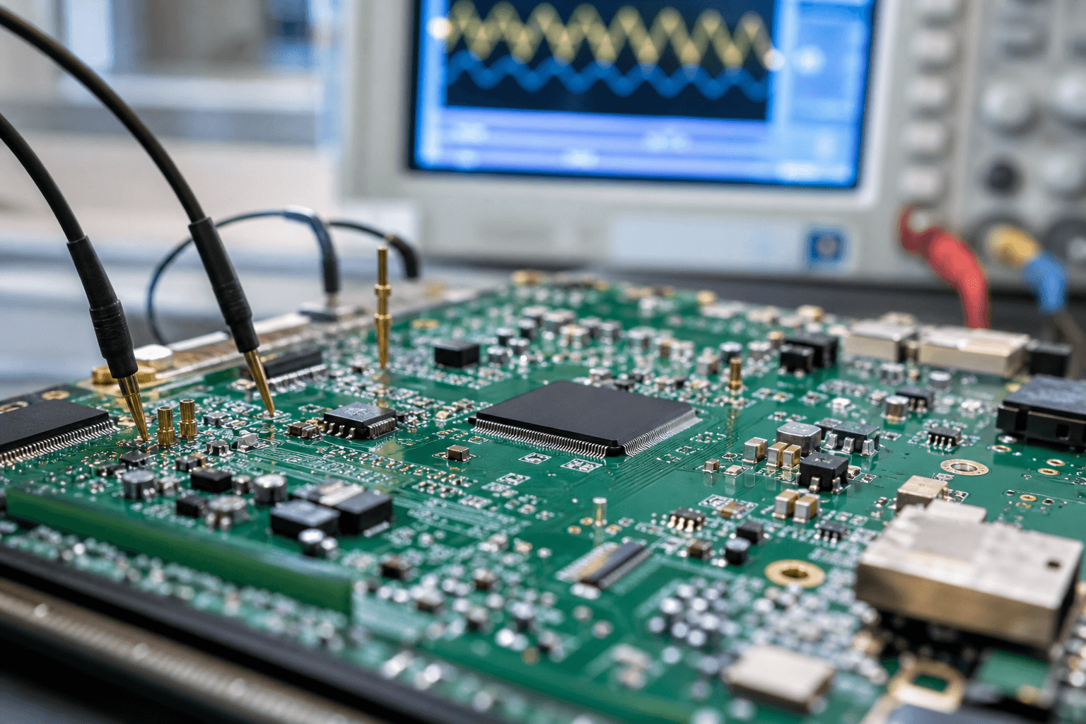
Design for manufacture only works as well as the data it is checked against. Generic DFM rules – minimum trace width, standard via sizes – catch the obvious problems. They do not catch the gap between your layout and the specific tolerances, panel sizes and documentation format your actual contract manufacturer needs.
A local design house that has run boards through Australian and New Zealand contract manufacturers before knows those specific tolerances already. That relationship-level knowledge is one of the more underrated cost savers in PCB design: it is the difference between a DFM review that says “this should be fine” and one that says “this CM’s solder mask process needs 0.15mm more clearance here, based on the last batch we ran with them.”
Zeus Design’s circuit board design and PCB layout service builds DFM review against the target manufacturer’s actual process capability into every layout stage, rather than treating it as a final checklist before file release.
Where Offshore Design-and-Build Packages Make Sense
Local is not automatically the right call for every project, and a fair comparison has to say so. Offshore design-and-build bureaus can be a reasonable fit when:
- The board is simple and low-risk. A straightforward two-layer board with no high-speed signals, no RF content and no compliance complexity has less to lose from a slower, lower-touch relationship.
- Volume production is the priority, not design iteration. If the design is already locked and stable, sourcing manufacturing offshore for cost at volume is a separate (and often sensible) decision from where the design work happens.
- Budget genuinely cannot support a local design engagement. Early-stage validation work on a tight budget may justify accepting slower iteration and weaker IP enforcement as a deliberate trade-off, as long as the team understands what it is trading away.
The trade-off to go in with eyes open about: Altium’s analysis of local versus offshore PCB prototyping notes that the per-unit cost advantage of offshore manufacturing often narrows or disappears once shipping, customs delays, and the cost of an extra board respin are factored in – particularly on a first prototype run where requirements are still settling.
A Practical Decision Framework
Rather than treating this as local-versus-offshore in the abstract, work through these questions for your specific project:
- How much does design iteration speed matter to your timeline? If requirements are still firming up, the time-zone cost of offshore design compounds with every change request.
- What is actually at risk if your design data leaks? A commodity sensor board carries different IP stakes to a board embodying genuine competitive advantage. Size the protection effort to the asset.
- Do you have a specific contract manufacturer already, or are you choosing one later? DFM is only as good as the manufacturer data it is checked against – local alignment matters more when the CM relationship already exists.
- Is this a one-off prototype or the first of many production runs? The cost of getting the first run wrong scales with how much is riding on it.
- Does the project need compliance sign-off (RCM, CE, FCC)? Local design teams familiar with Australian compliance pathways can plan for certification earlier, reducing redesign risk later.
For most funded hardware projects with real IP at stake and a production run on the horizon, this framework points toward local design with DFM tied to a known manufacturer – even where some downstream manufacturing volume is later sourced offshore for cost reasons.
Zeus Design’s Approach to Custom PCB Design in Australia
Zeus Design is an Australian-based electronics design house offering custom circuit board design and PCB layout as part of an integrated electronics design service. Engagements run discovery, schematic capture, multilayer layout and DFM review as a continuous process, with confidentiality agreements in place before any design data changes hands and DFM checked against the specific contract manufacturer your project will use.
For projects moving from a locked design into a working board quickly, Zeus Design’s rapid electronics and PCB prototyping service can take production-ready files through to a functional prototype for validation before a full production commitment. Where the product also needs embedded firmware or compliance planning, Zeus Design’s broader electronics design service covers that scope under the same team, so hardware and firmware decisions are made together rather than handed off cold.
If you are still deciding what to look for in a design partner more generally, see Zeus Design’s guide on how to choose PCB designers for your hardware project for a broader evaluation checklist that applies whether you go local or offshore.
FAQs
Is custom PCB design in Australia more expensive than offshore design?
Often yes on a like-for-like quote, but the comparison rarely stays like-for-like once iteration cycles, IP risk mitigation and respin probability are included. A local custom PCB Australia engagement typically front-loads cost into design quality and DFM discipline, which tends to reduce the chance of an expensive board respin later.
How do I protect my PCB design IP when working with any design partner?
Put a confidentiality agreement in place before sharing schematics, layout files or BOMs, and limit who receives the complete design package rather than partial blocks. This applies regardless of location, but enforcing the agreement is more straightforward when your design partner operates under Australian contract law. See IP Australia’s guidance on trade secrets and confidential information for the legal basis.
Can I design locally and still manufacture offshore for volume?
Yes, and this is a common hybrid approach. Many product teams keep schematic capture, layout and DFM with a local design house – where iteration speed and IP enforcement matter most – and separately source production manufacturing wherever it is most cost-effective once the design is locked and DFM-verified.
What should I ask a local PCB design house about their DFM process?
Ask which specific contract manufacturers they have run boards through recently, and whether DFM review is checked against that manufacturer’s actual process capability or against generic design rules. A design house with established local CM relationships should be able to name the tolerances they are designing to, not just the standards they reference.
Does local design help with compliance certification like RCM or CE?
It can. A local team familiar with the Australian compliance landscape is more likely to plan for RCM, CE or FCC requirements during schematic and layout stages, rather than discovering a compliance gap during pre-certification testing. Planning for certification early is consistently cheaper than redesigning for it after a failed test.
What is the biggest risk of offshore custom PCB design for a startup?
The combination of slower iteration and weaker practical IP enforcement is the biggest compounding risk, particularly for a first hardware product where requirements are still being refined. Each design change costs more in elapsed time, and if design data is exposed, recourse is harder to pursue across jurisdictions.
How long does a custom PCB Australia engagement typically take?
A straightforward two- to four-layer board with a complete requirements brief can reach Gerber handover in four to eight weeks with a local design partner. More complex multilayer boards with high-speed interfaces or RF content typically run eight to sixteen weeks. Local design does not inherently mean faster calendar time, but it tends to reduce the iteration delay within that timeline.
Next Steps
If your project carries real IP value, needs a production run rather than a one-off prototype, or has compliance requirements on the horizon, the case for a local custom PCB Australia engagement is strongest. If the board is simple, low-risk and the design is already stable, an offshore route may be a reasonable trade-off as long as you go in aware of what you are trading away.
Zeus Design works with Australian product teams on custom PCB design, DFM review and rapid prototyping as an integrated service. Get in touch to discuss where your project sits on this framework.
")


0 Comments