
A custom PCB design service covers every step between a product idea and a manufacturable circuit board – from requirements gathering and schematic capture through to multilayer layout, design-for-manufacture review and final Gerber file handover. For product teams and hardware startups who need more than an off-the-shelf module can offer, working with a specialist design partner is typically the fastest path to a board that performs reliably and scales to production without costly redesigns. This guide explains what the process involves, what to expect at each stage, and how to choose a partner who will keep your project on schedule.
TL;DR
- A custom PCB design service takes your requirements and delivers production-ready Gerber files, BOMs and assembly drawings.
- The process spans requirements gathering, schematic capture, multilayer layout, signal integrity review, DFM analysis and Gerber handover.
- Custom design is warranted when off-the-shelf modules cannot meet your size, power, performance or regulatory requirements.
- Key criteria for selecting a design partner include tool proficiency (Altium, KiCad), DFM experience, IPC compliance awareness and local support.
- Zeus Design delivers end-to-end circuit board design – schematic through to production-ready files – with integrated firmware and rapid prototyping support.
- Related services such as embedded firmware development and rapid prototyping are typically scoped alongside PCB design to avoid integration delays.
- Engaging a partner early – before component selection is locked – saves the most time and cost.
Who This Guide Is For
This guide is written for product managers, hardware engineers and founders who are either commissioning PCB design for the first time or evaluating whether their current design approach is fit for scale. It assumes you have a product concept and some understanding of the functional requirements but may not be familiar with what a professional design engagement looks like end to end.
If you are a startup moving from a breadboard prototype to a manufacturable board, or an established company spinning up a new product line, the process described here reflects what a quality Australian electronics design studio will deliver. Understanding each phase helps you brief a partner accurately, set realistic timelines and avoid the most common sources of project delay.
What a Custom PCB Design Service Covers
A well-structured custom PCB design engagement follows a repeatable sequence of phases. Each phase builds on the last, and skipping or compressing any of them is a common source of costly rework later in the project.
Requirements Gathering and Feasibility
Before a single schematic symbol is placed, a good design team will work through your functional and environmental requirements in detail. This includes power budget, operating temperature range, mechanical envelope (board dimensions and keep-out zones), connector and interface requirements, target component cost, and any applicable regulatory standards – for example, Standards Australia requirements for electrical safety or IPC design standards for PCB quality class.
This phase also surfaces feasibility concerns early. If a power rail topology will cause thermal issues at the target current, or if a target BOM cost is incompatible with the required component count, it is far better to resolve this before schematic capture begins.
Schematic Capture
The schematic is the logical blueprint of the circuit – it defines every component, its value, and how it interconnects with the rest of the design. A professional schematic is hierarchical, clearly annotated, and designed with the PCB layout phase already in mind. Power planes, decoupling strategy, and interface pinout decisions made at the schematic stage have a direct bearing on layout complexity and signal integrity.
Tools such as Altium Designer allow the schematic and layout to be tightly linked, reducing transcription errors and enabling real-time cross-probing during layout. Schematic review – ideally involving both the design engineer and a reviewer who was not the original author – is an essential quality gate before layout begins.
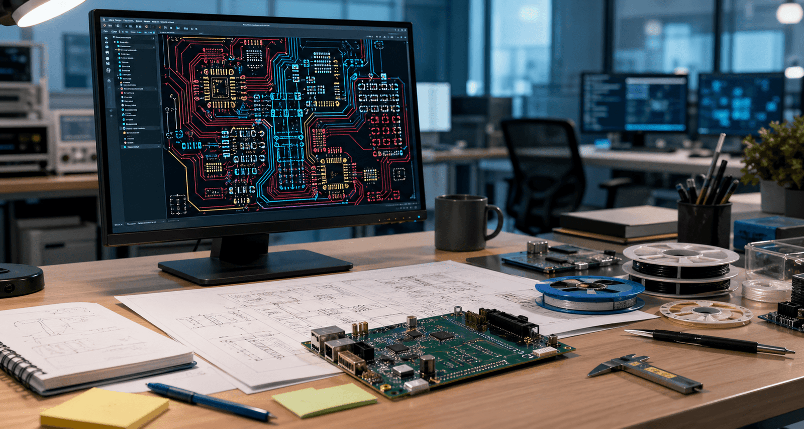
Multilayer PCB Layout
Layout translates the schematic into a physical board. For anything beyond a simple single-sided design, multilayer stackups are standard practice: two-, four-, six- and eight-layer boards each offer different trade-offs between cost, impedance control, signal integrity and EMC performance. A four-layer board with dedicated power and ground planes is a common starting point for mixed-signal IoT and industrial products.
Good layout practice includes controlled-impedance routing for high-speed signals, careful placement of decoupling capacitors close to power pins, thermal management for high-dissipation components, and EMC-aware techniques such as guard traces and split-plane avoidance. For RF and wireless designs, antenna placement and ground plane clearance are critical and must be validated against the chipset manufacturer’s reference design.
Design for Manufacture (DFM) Review
A PCB that looks correct in the CAD tool can still be difficult or expensive to manufacture if DFM considerations are ignored. DFM review checks that pad sizes, solder mask clearances, via dimensions, component spacing, and panelisation requirements align with the capabilities of your target contract manufacturer. Common DFM findings include pads that are too small for reliable soldering, components placed too close to board edges, or thermal relief that will cause cold solder joints on QFN pads.
Addressing DFM issues before files are released for fabrication avoids the most expensive form of rework: discovering manufacturing yield problems after your first production run.
Gerber File Handover and Production Documentation
The final deliverable package for a custom PCB design engagement typically includes Gerber files (RS-274X or Gerber X2 format), an NC drill file, a bill of materials (BOM), an assembly drawing (centroid/pick-and-place file), a schematic PDF, and any relevant test specifications. This package is what your PCB fabricator and assembly house require to manufacture and populate the board.
A thorough design partner will also provide a design review report summarising the decisions made, any constraints that were accepted as trade-offs, and recommendations for the prototyping phase.
Custom Design vs Off-the-Shelf Modules
Development boards and off-the-shelf modules – such as Arduino-compatible boards, ESP32 breakout boards or Raspberry Pi Compute Modules – are excellent for early prototyping and proof-of-concept work. However, they are rarely appropriate for a product that will be manufactured at any meaningful volume or that must meet specific size, power, cost or compliance requirements.
Custom PCB design becomes necessary when one or more of the following applies:
- Form factor constraints: Your product enclosure requires a board shape, thickness or connector placement that no off-the-shelf module can match.
- Power budget: Module-based designs often carry unnecessary circuitry that draws power and increases idle current beyond what battery-powered products can tolerate.
- BOM cost at volume: The premium you pay for the convenience of a module is priced in at unit one. At volumes above a few hundred units, a custom design almost always reduces per-unit cost significantly.
- Regulatory certification: A product that must carry CE, FCC or RCM marking typically requires a custom design with controlled RF characteristics and a declaration of conformity that cannot be inherited from a module’s own certification.
- Performance or reliability: When signal integrity, thermal performance or long-term component availability matter, a purpose-designed board gives you control that a module does not.
What to Look for When Selecting a Custom PCB Design Partner
The quality of a PCB design engagement is largely determined by the experience and process discipline of the team you engage. When evaluating design partners, consider the following:
Tool Proficiency and Design Process
Industry-standard EDA tools such as Altium Designer, KiCad and OrCAD each have different strengths. A partner who uses a professional, actively maintained tool and follows a documented design process – including schematic review gates and DFM checklists – is far less likely to deliver files with errors that cost you a board spin.
IPC Standards Awareness
The IPC publishes the PCB industry’s primary design and manufacturing standards, including IPC-2221 (generic PCB design standard), IPC-7351 (land pattern standard) and IPC-A-610 (acceptability of electronic assemblies). A partner who designs to IPC standards is designing to the same quality targets that professional contract manufacturers use – which means fewer surprises at the assembly stage.
DFM Experience with Australian CMs
If your product will be assembled in Australia or New Zealand, working with a design partner who has existing relationships with local contract manufacturers is a practical advantage. They will already know each CM’s specific capability tolerances, preferred panel sizes and documentation formats, which reduces back-and-forth between design and manufacturing.
Integrated Firmware Capability
Hardware and firmware are interdependent – decisions made in PCB layout (interrupt routing, peripheral assignment, debug header placement) directly affect firmware development. A design partner who can also develop the embedded firmware, or who has an established handover process for a separate firmware team, will deliver a more coherent result than one who treats PCB design as an isolated deliverable.
Local Communication and Support
Time zone alignment, prompt responses to technical questions and the ability to meet in person for design reviews are underrated project management factors. Australian-based design studios offer these advantages for local product teams in a way that offshore providers cannot reliably replicate.
Zeus Design’s Custom PCB Design Process and Deliverables
Zeus Design offers a complete circuit board design and PCB layout service covering every stage from requirements through to production-ready file delivery. The service is designed for product teams and hardware startups who need rigorous, well-documented engineering rather than a transactional file-delivery arrangement.
The Zeus Design PCB design engagement follows this sequence:
- Discovery and requirements definition – functional requirements, mechanical constraints, interface definitions, power budget, target cost and regulatory scope are documented before design work begins.
- Component selection and BOM strategy – components are selected for availability, long-term supply continuity and cost efficiency, with approved alternates identified where appropriate.
- Schematic capture in Altium Designer – hierarchical schematic design with internal peer review before layout sign-off.
- Multilayer PCB layout – stackup definition, controlled-impedance routing, EMC-aware placement and thermal management, with attention to IPC land pattern standards throughout.
- DFM review – layout reviewed against the capability specifications of the target contract manufacturer, with findings resolved before file release.
- Gerber and production documentation package – Gerber files, NC drill, BOM, assembly drawing and schematic PDF delivered as a complete production-ready package.
Zeus Design’s electronics design service also covers compliance planning and pre-certification design – a practical consideration for any product targeting RCM, CE or FCC approval. The design-for-manufacture approach is embedded throughout the process rather than treated as a final checklist, which reduces the likelihood of a second board spin being required for yield or assembly reasons.
Related Services: Prototyping, Electronics Design and Firmware
PCB design rarely exists in isolation. Most product development programmes also require:
- Rapid prototyping: Zeus Design’s rapid electronics and PCB prototyping service can take the completed PCB design files through to a functional prototype quickly – important for validation testing before committing to a production run.
- Embedded firmware development: For microcontroller-based designs, embedded firmware must be developed in parallel with or immediately after PCB design. Zeus Design’s firmware team works directly from the hardware specification, using the same design documentation produced during PCB design.
- IoT connectivity: For connected-device designs involving Wi-Fi, Bluetooth, cellular or LPWAN radios, antenna design, RF layout review and cloud integration planning are part of the broader electronics design scope.
- Test jig development: Production testing requires a test fixture designed to interface with the PCB under test. Scoping this alongside PCB design avoids the common situation where test points are inaccessible or missing from the final layout.
Engaging these services as part of a coordinated scope, rather than commissioning them sequentially from separate suppliers, is one of the most effective ways to reduce total project time and integration risk.
FAQs
How long does a custom PCB design project take?
Timeline depends on board complexity, layer count and the completeness of the initial requirements. A straightforward two- to four-layer design for a well-defined product can reach Gerber handover in four to eight weeks. Complex multilayer designs with high-speed interfaces, RF content or significant component count typically take eight to sixteen weeks. Incomplete or frequently changing requirements are the most common cause of timeline overruns, so investing in a thorough discovery phase pays dividends.
What information do I need to provide at the start of a PCB design engagement?
A good design partner will help you structure the brief, but the more detail you can provide upfront the better. Useful inputs include a functional block diagram, interface and connector requirements, mechanical envelope or CAD model, power supply specification, target component cost per unit, approximate production volume and any relevant regulatory requirements. Reference designs or previous design files are also helpful if they exist.
What is the difference between schematic design and PCB layout?
The schematic is the logical representation of the circuit – it shows every component and how it connects electrically, without reference to physical position on the board. PCB layout translates that schematic into a physical board design, defining where each component sits, how copper traces route between them, which signals run on which layers, and how the board will be manufactured. Both phases are required, and errors in the schematic propagate directly into the layout.
What files are delivered at the end of a PCB design project?
A standard production documentation package includes Gerber files (one per copper layer, plus solder mask, silkscreen and board outline), an NC drill file, a bill of materials with manufacturer part numbers and approved alternates, an assembly drawing with component placement and orientation, a centroid file for pick-and-place programming, and a schematic PDF. Some engagements also include a design review report and test specification.
How does design for manufacture (DFM) affect my project?
DFM review compares the completed layout against your target contract manufacturer’s process capabilities – minimum trace width, via drill size, pad-to-edge clearance, thermal relief requirements and panelisation constraints. Catching DFM issues before file release avoids expensive board respins and production yield problems. A design partner with existing CM relationships can run DFM checks against the specific capabilities of the facility that will build your boards, rather than against generic design rules.
Can Zeus Design also handle firmware development for the PCB?
Yes. Zeus Design offers integrated embedded firmware and software development alongside PCB design. Co-developing hardware and firmware from the same technical specification – rather than handing a finished PCB to a separate firmware team – reduces integration issues and typically shortens overall project time. Peripheral assignment, interrupt mapping and debug interface decisions can be made collaboratively when hardware and firmware engineers are working in the same team.
What is the IPC standard and why does it matter for PCB design?
IPC is the global trade association for the printed electronics industry and publishes the primary standards governing PCB design, manufacturing and assembly quality. Key standards include IPC-2221 for generic design requirements and IPC-7351 for land pattern geometry. Designing to IPC standards means your PCB is being designed to the same quality targets that professional assembly houses use as acceptance criteria – which reduces the risk of manufacturing defects and makes it easier to qualify alternative contract manufacturers if needed.
Start Your Custom PCB Design Project
Whether you are moving a proof-of-concept to a production-ready board or starting a new hardware product from requirements, Zeus Design’s custom PCB design service covers the full journey – from schematic through to Gerber handover – with integrated DFM, firmware support and rapid prototyping available alongside.
The earlier you engage a design partner in the product development process, the more influence they can have on cost, timeline and manufacturability. Contact the Zeus Design team to discuss your requirements.
")


0 Comments