
Circuit board design is the engineering process that turns an electrical concept into a manufacturable printed circuit board – and for founders or product companies new to hardware, it is usually the most technically demanding step in bringing a physical product to market. This guide walks through every major stage of the process: schematic capture, component selection, layer stack planning, PCB layout, signal integrity, design for manufacture (DFM), and the manufacturing files your fabricator needs to build your board. Whether you are building a consumer IoT device, industrial equipment, or a medtech prototype, understanding how the process works helps you make better decisions, ask better questions, and avoid the costly mistakes that derail hardware timelines.
TL;DR
- Circuit board design covers schematic capture, component selection, PCB layout, DFM review, and generating Gerber/BOM/assembly files for manufacturing.
- Schematic errors are far cheaper to fix before layout begins – the later a mistake is caught, the more it costs.
- Layer count, material choice, and trace geometry all affect signal integrity, EMC performance, and fabrication cost.
- Design for manufacture (DFM) rules should be applied throughout the layout phase, not bolted on at the end.
- Component selection must account for lead times, pricing at volume, and availability – not just electrical spec.
- Manufacturing files are a package: Gerber files, drill files, BOM, pick-and-place (centroid) file, and assembly drawings.
- Working with an experienced PCB design partner like Zeus Design reduces rework cycles and compresses time to prototype.
Who This Guide Is For
This guide is written for founders, product managers, and early-stage hardware companies who are evaluating the circuit board design process for the first time. You do not need an engineering background to follow it. The goal is to give you enough working knowledge to manage a PCB design project intelligently – whether you are hiring an in-house engineer, engaging a design partner, or trying to understand what your team is telling you.
If you have already shipped hardware, much of this will be review. Skip to the sections on DFM, common mistakes, or Zeus Design’s services if you want the practical detail most relevant to your situation.
What Circuit Board Design Involves
A printed circuit board is a layered structure of copper conductors and insulating substrate that physically connects and mechanically supports electronic components. Circuit board design is the process of specifying those connections and producing the files that allow a fabricator to manufacture the board and an assembler to place components on it.
At a high level, the process involves six interconnected activities:
- Schematic capture – defining what components are in the circuit and how they are electrically connected
- Component selection – choosing specific parts that meet the electrical spec, are available in volume, and are cost-effective to assemble
- Layer stack planning – deciding how many copper layers the board needs and how they are arranged
- PCB layout and routing – placing components on the board and drawing copper traces to connect them
- DFM review – verifying that the design can be fabricated and assembled reliably and economically
- Manufacturing output – generating Gerber files, a bill of materials (BOM), drill files, and assembly data
Each of these activities has its own rules, tradeoffs, and failure modes. The sections below explain each one in plain language.
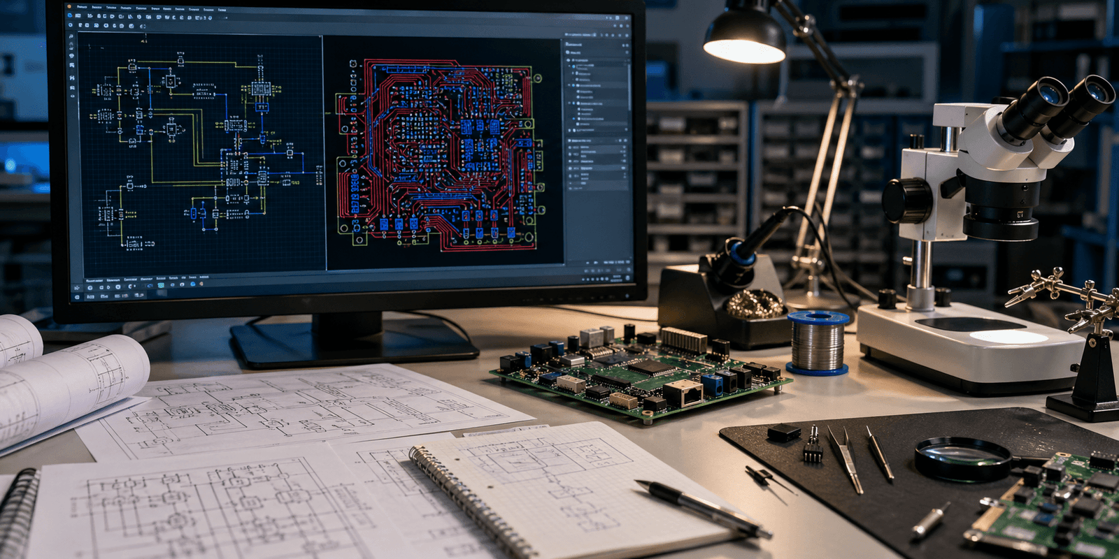
Stage 1: Schematic Capture
The schematic is a logical diagram of the circuit. It shows every component – microcontrollers, power regulators, connectors, passive components – and every electrical connection between them. It does not show how components are physically arranged on the board; that comes later in layout.
A well-structured schematic is hierarchical: power, ground, digital signals, analogue signals, and communication interfaces are kept visually distinct. This makes it easier to review, debug, and hand off to another engineer. Tools like Altium Designer, KiCad, and Cadence OrCAD are commonly used for professional schematic capture.
According to IPC-2221, the generic standard for printed board design, schematic review is the most cost-effective point at which to catch errors. A mistake found in schematic costs minutes to fix; the same mistake found after fabrication costs a board revision, additional fabrication fees, and weeks of delay.
Key schematic quality checks include:
- All power rails correctly decoupled with appropriate capacitors
- Reset, boot, and configuration pins handled per the datasheet
- Communication interfaces (SPI, I2C, UART, USB) with correct pull-ups, termination, and ESD protection
- Correct pinout for every connector and IC package
- Electrical rules check (ERC) run and all warnings resolved or documented
Stage 2: Component Selection
Choosing components is not just an electrical exercise – it is a supply chain decision. A component that meets your spec perfectly but has a 52-week lead time from a single supplier is a risk to your entire programme.
Professional electronics design practices account for:
- Multi-sourcing – specifying at least two approved manufacturers for every critical component
- Lifecycle status – avoiding components already flagged as end-of-life or not recommended for new designs (NRND)
- Package selection – choosing packages that are compatible with your assembler’s pick-and-place capabilities and inspection equipment
- Pricing at volume – running the BOM cost at 100, 1,000, and 10,000 units so you understand the cost curve before you commit to a design
Component selection directly affects the manufacturability and long-term supportability of your product. Founders building hardware for the first time often underestimate how much time experienced engineers spend on this step.
Stage 3: Layer Stack and Board Constraints
A PCB is built from alternating layers of copper and dielectric (insulating) material. Simple boards may use two layers (top and bottom copper). More complex products – those with high-speed digital interfaces, RF, or high-density component layouts – typically require four, six, or more layers.
Layer stack decisions affect:
- Signal integrity – controlled impedance traces for high-speed signals need a reference plane at a defined distance
- EMC – proper ground planes reduce electromagnetic emissions and improve immunity
- Thermal management – internal copper layers can serve as thermal spreading layers
- Cost – each additional layer pair adds fabrication cost
The board outline (mechanical dimensions), minimum trace width, minimum via size, and copper-to-edge clearances are also defined at this stage, typically in a design constraints document that guides the layout engineer.
Stage 4: PCB Layout and Routing
PCB layout is where the schematic becomes a physical board. The layout engineer places components on the board and routes copper traces between them according to the schematic netlist and the design constraints established earlier.
Good layout practice includes:
- Component placement strategy – placing components to minimise trace length for critical signals, group related circuits, and leave room for assembly and test access
- Power distribution – using wide traces or copper pours for power and ground to minimise voltage drop and inductance
- Differential pair routing – keeping paired traces equal in length and tightly coupled for USB, Ethernet, LVDS, and similar interfaces
- Via usage – minimising via stubs on high-speed signals and using via-in-pad where required for fine-pitch BGAs
- Copper pours and ground stitching – filling unused copper areas with ground and stitching planes together with vias to reduce EMC risk
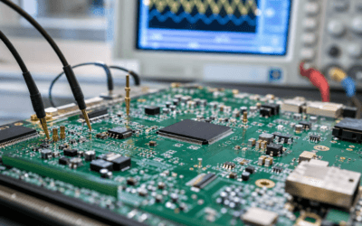
Design rule check (DRC) is run continuously during layout to catch clearance violations, unrouted connections, and constraint violations before they reach fabrication.
Stage 5: Design for Manufacture (DFM)
DFM is the practice of designing a board so it can be fabricated and assembled reliably, cost-effectively, and at the quality level your product requires. DFM is not a single review at the end – it should be applied throughout the layout phase.
Common DFM considerations include:
- Pad geometry and courtyard clearances – pads sized and spaced to suit reflow, wave, or selective soldering processes
- Tombstoning prevention – symmetric thermal connections on small two-terminal components
- Solder mask – apertures sized correctly relative to copper pads to prevent bridging and solder balling
- Panelisation – boards designed for panel assembly with appropriate breakaway tabs, fiducial marks, and orientation markers
- Testability – test pads placed for in-circuit test (ICT) or flying-probe access
IPC-7711/7721 provides industry-standard guidance on repair and rework, which is a useful lens for evaluating how DFM-friendly a design is. Engineers Australia also publishes practice notes relevant to electronics design quality for Australian practitioners.
Stage 6: Manufacturing Output Files
When layout is complete, the design is exported as a manufacturing package. This typically includes:
- Gerber files (RS-274X) – one file per copper layer, plus solder mask, silkscreen, and board outline
- Drill file (Excellon) – hole sizes and positions for through-hole vias and components
- Bill of materials (BOM) – a structured list of every component with reference designator, description, manufacturer part number, and quantity
- Pick-and-place (centroid) file – X/Y coordinates and rotation for each component, used to programme the pick-and-place machine
- Assembly drawing – a document showing component placement, polarity marks, and any special assembly instructions
The quality of manufacturing output files directly affects the accuracy of fabricator quotations and the smoothness of first-article inspection. Poorly formatted or incomplete manufacturing packages are a common source of delay at production entry.
Common Mistakes and How to Avoid Them
Most PCB design problems are predictable. Here are the mistakes that most frequently affect founders and early-stage hardware teams:
Skipping or rushing the schematic review
Layout is time-consuming. When timelines are tight, teams are tempted to start placing components before the schematic is properly reviewed. This almost always produces a board revision. Invest the time upfront – a structured schematic review against the datasheet, a checklist, and an independent technical review is the highest-ROI activity in the PCB design process.
Not running DRC and ERC continuously
Design rule checks and electrical rules checks are most useful when they are run throughout the design process, not just at the end. Modern EDA tools support live DRC – use it. Treating DRC as a final-step formality means that violations accumulate and become harder to diagnose.
Ignoring component availability during design
Specifying a single-source component or a part with limited stock is a supply chain risk that can stall your programme for months. Check availability on Digi-Key, Mouser, and LCSC at the component selection stage, not after the layout is complete.
Underspecifying the manufacturing files package
Sending a fabricator only Gerber files without a BOM, pick-and-place file, or assembly drawing leads to back-and-forth that delays production entry. Agree the manufacturing output package with your contract manufacturer before the design is complete.
Treating EMC as an afterthought
Electromagnetic compatibility is far easier to address in layout than in a redesign. Correct return path management, decoupling placement, filter routing, and cable connector layouts add minimal effort during design but can mean the difference between passing and failing pre-compliance testing.
Zeus Design’s Circuit Board Design Service
Zeus Design’s circuit board design service covers the complete PCB design process for Australian and international product companies – from schematic capture through to production-ready manufacturing files. The team uses Altium Designer for schematic and layout, with a structured review process at each stage of the design.
The service includes:
- Schematic capture and electrical review against datasheet requirements
- Component selection with multi-source and lifecycle verification
- Layer stack planning for signal integrity, EMC, and cost targets
- PCB layout with DFM rules applied throughout
- Pre-compliance EMC design practices
- Complete manufacturing output: Gerber files, BOM, pick-and-place file, and assembly drawing
- DFM review with your contract manufacturer prior to production entry
Zeus Design works with founders from the earliest stages of hardware development, including clients who are approaching circuit board design for the first time. The team can engage at the schematic phase, take over an existing layout, or run the full process from concept to manufacturing files – depending on where you are in your programme.
Related Services
Circuit board design rarely sits in isolation. Most hardware products require a broader set of capabilities to reach market. Zeus Design offers these adjacent services alongside its PCB design work:
Electronics Design
Electronics design covers the end-to-end hardware development process: circuit design, PCB layout, firmware integration, compliance planning, DFM, cost optimisation, and test system development. If you need a partner who can manage the full hardware programme rather than just the PCB files, the electronics design service is the right starting point.
Rapid Prototyping
Rapid prototyping is Zeus Design’s quick-turn service for producing functional PCB prototypes and proof-of-concept builds. Once circuit board design files are complete, rapid prototyping gets a physical board in your hands quickly – so you can validate the design, identify issues early, and move to the next iteration or production without waiting on standard fabrication lead times.
Embedded Software Development
Electronics hardware is only half the product for most connected devices. Zeus Design’s embedded software team develops firmware and embedded software alongside the PCB design, ensuring that the software architecture matches the hardware from the start – not after you have received prototype boards and discovered integration problems.
FAQs
How long does circuit board design take?
A simple two-layer board with a known architecture can be schematic-captured and laid out in two to four weeks. A complex multilayer board with high-speed interfaces, RF, or BGA components typically takes six to twelve weeks including review cycles. These timelines assume a complete and stable specification – changes to requirements after layout has begun are the most common cause of delay.
How much does circuit board design cost?
PCB design cost varies significantly with complexity. Simple two-layer boards for straightforward applications may be quoted from a few thousand dollars in engineering time. Complex multilayer boards with high-speed interfaces, RF, or dense component layouts can run to tens of thousands of dollars. Manufacturing cost is a separate line item – it depends on layer count, board size, quantity, and assembly complexity. The best way to get an accurate number is to share your requirements and receive a scoped quote.
What is the difference between schematic design and PCB layout?
Schematic design defines what is in the circuit and how the components are electrically connected – it is a logical diagram. PCB layout translates that logical diagram into a physical board, placing components in specific locations and routing copper traces between them. Both steps are required to produce a manufacturable board, and errors in the schematic propagate into the layout if not caught early.
What files do I need to give a PCB manufacturer?
A complete manufacturing package includes Gerber files (one per copper layer, solder mask, and silkscreen), a drill file in Excellon format, a bill of materials with manufacturer part numbers, a pick-and-place (centroid) file for component placement, and an assembly drawing. Some fabricators also request a fabrication drawing specifying board thickness, surface finish, and impedance requirements. Providing an incomplete package is a common source of quotation errors and production delays.
How many PCB layers does my product need?
Layer count depends on component density, signal speed, power requirements, and EMC targets. Many simple products work well on a two-layer board. Products with microprocessors, wireless connectivity, or multiple power domains typically benefit from four layers – two signal layers and two dedicated power/ground planes. High-speed digital interfaces, RF designs, and dense BGA layouts often require six or more layers. Your design engineer should recommend a layer stack based on your specific requirements.
What is DFM and why does it matter?
Design for manufacture (DFM) is the practice of designing a PCB so it can be fabricated and assembled reliably and economically. DFM covers pad geometry, solder mask design, component spacing, panelisation, and testability. Boards without proper DFM review often produce assembly defects – solder bridges, tombstoned components, poor solder joints – that reduce yield and increase rework cost. DFM issues caught before fabrication are orders of magnitude cheaper to fix than those found during assembly or test.
Can Zeus Design take over an existing PCB design?
Yes. Zeus Design regularly inherits designs at various stages of completion – from partially completed schematics through to layouts that need DFM improvement before production entry. The starting point is a design review to assess what is complete, what needs to be revised, and what files are available. From that review, a scope and timeline can be agreed. Existing designs in Altium format are the most straightforward to take over; other formats can typically be imported or recreated.
Conclusion
Circuit board design is a disciplined engineering process – one that rewards careful upfront work and punishes shortcuts. For founders building hardware for the first time, the most important insight is that mistakes caught in schematic review cost far less than mistakes caught in prototype testing, and mistakes caught in prototype testing cost far less than mistakes caught at volume production. The investment in getting the process right from the beginning is almost always the faster and cheaper path.
Zeus Design works with Australian and international product companies on the full circuit board design process – from initial schematic through to production-ready manufacturing files. If you are starting a new hardware programme or need a second opinion on a design in progress, get in touch to discuss your project.
")


0 Comments