
Electronics design is the end-to-end engineering discipline that transforms a product concept into manufacturable, compliant hardware – and for Australian hardware startups and product companies, choosing the right design partner can determine whether a product reaches market on time or stalls in expensive revision cycles. This guide covers the complete electronics design process: what it involves, when you need specialist support, what risks to manage, and how a local full-service firm like Zeus Design can carry a project from early concept through to production-ready deliverables.
TL;DR
- Electronics design spans circuit design, PCB layout, firmware integration, compliance planning, and design for manufacture (DFM) – it is not just PCB layout.
- Australian hardware products must meet ACMA regulatory requirements and carry RCM marking before going to market; this needs to be designed in, not bolted on.
- Rapid prototyping early in the process compresses validation cycles and catches design errors before production tooling is committed.
- Firmware and embedded software developed alongside hardware – rather than after – reduces integration risk and shortens time to market.
- DFM (design for manufacture) reviews, component selection, and BOM optimisation directly affect unit production cost and supply chain resilience.
- A local Australian electronics design partner offers faster iteration, clearer communication, and accountability that offshore-only engagements rarely match.
- Zeus Design provides a complete electronics design service covering hardware, firmware, prototyping, and production handover from its Sydney-based team.
The Commercial Problem Australian Hardware Companies Face
Australia has a strong pipeline of hardware innovation – industrial IoT, medical devices, agricultural technology, consumer electronics, and defence-adjacent products – but a relatively small pool of specialist electronics design firms capable of taking a product all the way from whiteboard to factory floor.
The result is a fragmented landscape where companies piece together a schematic designer here, a PCB layout contractor there, and a firmware developer working in isolation. This hand-off model introduces integration gaps, communication overhead, and compliance blind spots that push out timelines and drive up cost.
According to the Department of Industry, Science and Resources, Australian technology exports have grown consistently – creating commercial pressure on local hardware companies to ship faster and more reliably than ever before. For product teams without an in-house electronics engineering function, the design partner they choose is effectively their entire hardware engineering department.
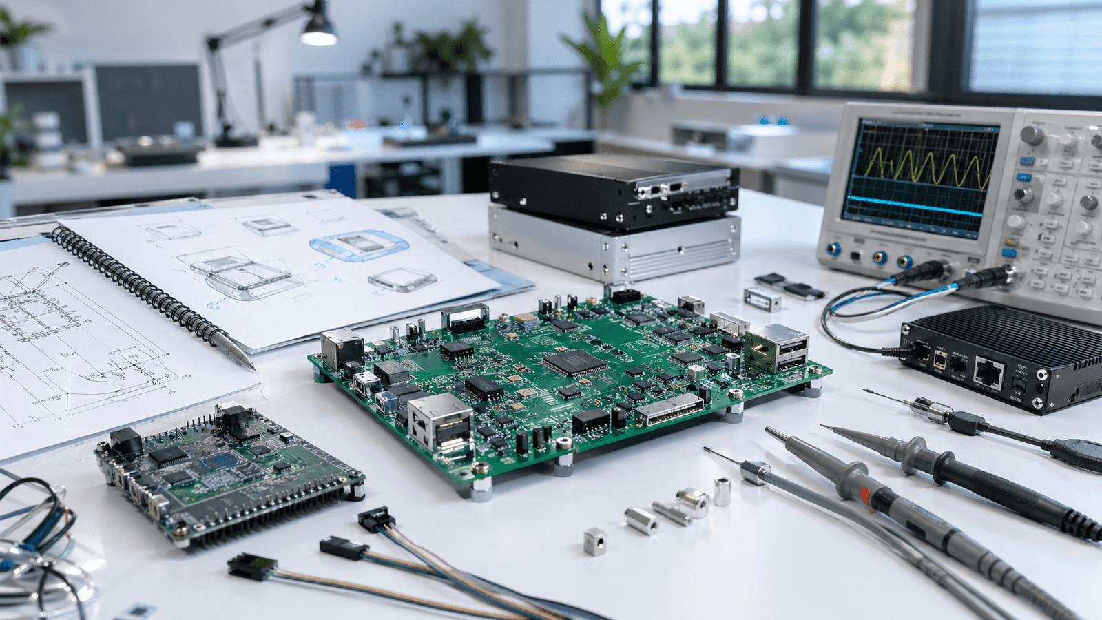
What Electronics Design Services Include
A full-service electronics design engagement covers considerably more than drawing schematics. The major workstreams are:
Circuit and Schematic Design
The foundation of any hardware product. Covers component selection, analog and digital circuit design, power supply architecture, signal integrity planning, and protection circuitry. Good schematic design at this stage prevents expensive redesigns downstream.
PCB Layout and Design
PCB design and layout translates the schematic into a physical board. This involves layer stackup decisions, component placement, impedance-controlled routing for high-speed signals, thermal management, and EMC-aware layout practices. Multilayer boards, HDI designs, and RF-sensitive layouts each require specialist handling.
Firmware and Embedded Software Development
Hardware without firmware is inert. Embedded software development covers bare-metal and RTOS-based firmware for microcontrollers and microprocessors, bootloaders, hardware abstraction layers, communication stacks (UART, SPI, I2C, USB, CAN), and wireless protocol integration (Wi-Fi, Bluetooth, LTE-M, LoRaWAN). Co-developing firmware with hardware – rather than after – catches pin assignment conflicts and power budget issues early.
Prototyping and Validation
Functional prototypes allow the engineering team to validate circuit behaviour, test firmware integration, assess thermal performance, and identify mechanical fit issues before production tooling is ordered. Rapid electronics prototyping compresses this cycle significantly – getting working boards into engineers’ hands in days rather than weeks.
Compliance and Certification Planning
Products sold in Australia must carry RCM (Regulatory Compliance Mark) certification, which covers electrical safety and electromagnetic compatibility (EMC). Wireless products face additional spectrum licensing obligations managed by the Australian Communications and Media Authority (ACMA). Compliance should be designed in from the start – not addressed as an afterthought that forces board respins.
Design for Manufacture (DFM)
DFM reviews examine whether a design can be assembled, tested, and reworked efficiently at volume. This covers component package choices, paste apertures, fiducial markers, test point placement, panellisation, and assembly tolerances. A board that is difficult to manufacture reliably will bleed cost at every production run.
Test Systems and Jigs
Production test fixtures enable rapid, repeatable functional testing of assembled boards before they leave the factory. Investing in a well-designed test jig early reduces field return rates and builds a quality feedback loop into the manufacturing process.
When a Project Needs Electronics Design Support
Not every project requires end-to-end design services. The situations that most commonly benefit from specialist support are:
- New product development: A startup or product company bringing a hardware concept to market for the first time, with no internal electronics engineering capability.
- Product redesign or cost reduction: An existing product where the BOM cost is too high for target margins, or where a key component has been discontinued and the design needs re-architecture.
- IoT connectivity addition: An established product that needs wireless communication, cloud connectivity, or sensor integration added to an existing hardware platform.
- Compliance remediation: A product approaching market entry that has failed pre-compliance testing and needs circuit or layout changes to pass EMC or safety requirements.
- Scaling from prototype to production: A proof-of-concept that has been validated but needs DFM review, production-grade PCB layout, and test system development before volume manufacturing begins.
- Firmware-hardware integration: A hardware design that exists but lacks the embedded software to make it functional, or where firmware from a previous contractor does not meet reliability or performance requirements.
Technical and Commercial Risks to Manage
Electronics design projects carry a predictable set of risks. Addressing them proactively is far cheaper than discovering them in production.
Component Availability and Obsolescence
The global semiconductor supply chain remains volatile. Designing around components with long lead times, single-source supply, or approaching end-of-life status creates production fragility. Good component selection practice includes identifying second-source alternatives and avoiding specifying parts that have announced last-time-buy dates. The International Electrotechnical Commission (IEC) publishes guidance on component lifecycle management that informs best practice.
EMC Failures Late in Development
Electromagnetic compatibility failures at the pre-compliance or accreditation testing stage are among the most costly surprises in hardware development. They typically require PCB layout changes, component additions, or shielding – all of which mean board respins and additional test cycles. EMC-aware design from the schematic stage (careful ground plane management, differential pair routing, filter placement, decoupling strategy) reduces this risk materially.
Thermal Management
Power electronics, RF components, and high-performance microprocessors generate heat that must be managed or the product will fail in field conditions. Thermal simulation and thermal relief design in the PCB layout stage costs a fraction of a field recall.
Firmware Reliability and Security
Connected hardware products carry cybersecurity obligations. The Australian Cyber Security Centre’s Information Security Manual sets the benchmark for connected device security posture in Australia. Secure boot, over-the-air (OTA) update mechanisms, encrypted communication, and credential management need to be specified at the firmware architecture stage – retrofitting security to firmware that was not designed for it is expensive and often incomplete.
DFM Oversights
A board that tests perfectly at prototype stage can be unmanufacturable at volume if DFM has not been applied. Common issues include insufficient clearances for pick-and-place nozzles, paste bridges on fine-pitch components, and missing test access. These issues do not surface until the first production run – at which point the cost of the respun board is accompanied by delayed customer commitments.
Zeus Design’s Electronics Design Process
Zeus Design operates as a full-service electronics design firm from Sydney, Australia. The engagement process is structured to carry projects through every phase without hand-off gaps:
Phase 1 – Requirements and Architecture
A detailed technical brief is developed covering performance requirements, power budget, connectivity requirements, mechanical constraints, target production cost, regulatory obligations, and timeline. This brief drives all subsequent design decisions and provides the benchmark against which design choices are evaluated.
Phase 2 – Circuit Design and Schematic Capture
Component selection, power supply architecture, protection and filtering, and full schematic capture. Key design decisions are documented with the rationale, enabling future engineers (and production partners) to understand why the design is the way it is.
Phase 3 – PCB Layout and Design Review
Layout proceeds in parallel with early firmware work. A formal design review is conducted before Gerber release – covering signal integrity, EMC layout rules, DFM checks, and a bill-of-materials review for component availability. Zeus Design’s PCB design service uses Altium Designer and maintains a full design history for revision traceability.
Phase 4 – Rapid Prototyping and Bring-Up
Prototype boards are fabricated and assembled, then brought up systematically – power rails verified, clocks checked, communication interfaces validated, and firmware loaded. Issues found at this stage are resolved before the design is locked for production. Zeus Design’s rapid prototyping service supports quick-turn builds that keep development timelines moving.
Phase 5 – Firmware Integration and System Testing
Embedded firmware is developed and integrated on the prototype hardware. System-level testing validates that the hardware and firmware together meet the requirements brief – including communication protocols, power modes, failure handling, and security features.
Phase 6 – DFM Review and Production Handover
Before production, a DFM review is conducted with the manufacturing partner. Assembly drawings, a complete bill of materials, production test specifications, and Gerber files are packaged into a production-ready design package. Test jig requirements are specified and, where required, designed and built in-house.
How Electronics Design Connects to Related Services
Few hardware products are electronics alone. The most successful product launches integrate electronics design with adjacent disciplines from the outset:
Firmware and Embedded Software
Hardware and firmware are interdependent. Zeus Design’s embedded software development service works in parallel with electronics design so that pin assignments, power modes, and communication interfaces are validated against real firmware requirements before the PCB is finalised.
IoT Cloud Connectivity
Connected hardware products need a backend. Cloud architecture, device provisioning, OTA update infrastructure, and real-time data pipelines need to be specified alongside the hardware design – not after it ships. Zeus Design’s cloud development practice works with the electronics team to ensure the hardware design supports the cloud architecture it needs to connect to.
Mobile Applications
Many hardware products pair with iOS or Android apps for configuration, monitoring, or control. Designing the Bluetooth or Wi-Fi interface specification in concert with the app team – rather than handing over a fixed hardware interface spec after the board is committed – results in a better user experience and fewer integration surprises.
Rapid Prototyping
For earlier-stage projects where the concept has not yet been fully validated, Zeus Design’s rapid prototyping service provides a lower-cost entry point – building a functional proof of concept to validate the core technical thesis before committing to a full production-grade electronics design engagement.
FAQs
How long does an electronics design project take?
Timeline depends on complexity. A straightforward single-board design with established connectivity requirements and no unusual certification obligations can move from brief to production-ready design package in 10-16 weeks. Complex multi-board systems, RF-heavy designs, or products with demanding compliance requirements typically require 20-36 weeks. Rapid prototyping phases can run in parallel to compress the overall timeline.
How much does electronics design cost in Australia?
Electronics design is priced as a professional engineering engagement – not a commodity service. A typical end-to-end project (circuit design, PCB layout, firmware integration, prototyping, DFM review) for a moderately complex product ranges from $30,000 to $150,000 AUD depending on scope, complexity, and the number of prototype iterations required. Projects that invest properly in design quality upstream consistently achieve lower unit production costs and fewer field issues.
Do I need a full electronics design engagement or just PCB layout?
If you have a complete, reviewed schematic and a clear component specification, standalone PCB layout may be sufficient. However, most early-stage products benefit from a fuller engagement – circuit design errors that reach the layout stage are far more expensive to fix than those caught at the schematic review. A brief scoping conversation will clarify which scope is appropriate for your project.
What Australian compliance requirements apply to electronics products?
Products sold in Australia must carry RCM (Regulatory Compliance Mark) certification, which covers both electrical safety (managed by state electrical regulators) and electromagnetic compatibility (managed by ACMA). Products that include wireless radios must comply with ACMA’s licence-exempt framework or hold appropriate spectrum licences. Medical devices face additional obligations under the Therapeutic Goods Administration (TGA). Compliance requirements should be identified at the requirements phase and designed into the product – not addressed after the design is complete.
Can Zeus Design manage manufacturing as well as design?
Zeus Design’s core service is electronics design, firmware development, and prototyping. For production manufacturing, Zeus Design works with established Australian and international manufacturing partners and can manage the handover process – including production design packages, test fixture specifications, and supplier qualification – so clients are not left to navigate manufacturing alone after the design is complete.
What happens if the prototype fails testing?
Prototype failures are a normal and expected part of the development process. Zeus Design documents the failure mode, identifies the root cause (circuit error, layout issue, firmware bug, or requirements misunderstanding), implements a fix, and re-spins the affected boards. The goal of rapid prototyping is precisely to catch these failures early – before production tooling is committed – so that each iteration is a controlled step forward rather than a costly setback.
Is local Australian electronics design better than using an offshore firm?
Offshore electronics design can offer lower headline rates, but the total cost of engagement often converges once communication overhead, time-zone friction, IP risk, and rework costs from misunderstood requirements are factored in. For Australian products that need to meet local regulatory requirements, navigate Australian supply chains, and iterate quickly, a local design partner – accountable and reachable – typically delivers a better outcome. Australian-made design documentation also supports local manufacturing and service relationships over the product’s commercial life.
")


0 Comments