

Printed Circuit Boards (PCBs) form the core of modern electronic devices, from smartphones and computers to industrial machinery. Mastering PCB design best practices is essential for creating reliable, high-quality electronics that meet technical and regulatory requirements. By focusing on elements like signal integrity, grounding, thermal management, and testing, designers can ensure their PCBs perform optimally in real-world conditions. Applying these practices enhances both innovation and reliability in today’s rapidly advancing electronics industry.
In this guide, we’ll explore the best practices for designing a PCB Layout to help you design PCB layouts for modern electronics.
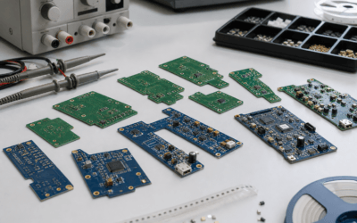
What is a PCB? Basics of Printed Circuit Boards
A PCB (Printed Circuit Board) is a board that physically supports and connects electronic components via etched copper pathways, also known as traces. These pathways allow electrical signals to flow, enabling the device to function as intended. PCB design involves arranging these pathways and components for maximum efficiency, reliability, and functionality. Understanding these basics is crucial for engineers and designers who want to master PCB design.
PCB design has evolved from manual wiring to highly sophisticated layouts optimized for today’s high-tech devices. Modern PCB circuit board design must balance functionality, size, and complexity, as electronics become smaller and more powerful. The evolution of PCB design reflects these advances, with engineers constantly innovating to keep up with the latest demands in areas like IoT, telecommunications, and consumer electronics.
Key Elements in Designing a PCB Layout
Designing an effective PCB involves understanding the various components that work together to create a functional circuit:
- Components and Traces: The PCB layout includes components like resistors, capacitors, and integrated circuits (ICs), all interconnected by copper traces. These traces carry electrical signals between components, and their arrangement impacts the board’s functionality.
- Accurate Schematics: Before laying out the board, creating an accurate schematic diagram is essential. Schematics serve as blueprints, guiding the placement of components and ensuring all electrical connections align with design specifications.
Grasping these foundational elements lays the groundwork for effective PCB layouts, supporting functionality and enhancing product performance.
Best Practices For PCB Layout Design
Mastering PCB design requires following best practices that ensure reliability, functionality, and compliance. Here are some essential tips to consider:
1. Maintain Signal Integrity
Signal integrity is critical for preventing issues like crosstalk, timing errors, and signal degradation, which can compromise performance. Careful layout planning, such as maintaining adequate spacing between traces, helps avoid signal interference. High-speed designs, in particular, benefit from a focus on signal integrity to ensure stable operation in real-world applications.
2. Implement Effective Grounding Strategies
Proper grounding is a fundamental best practice in PCB design, minimizing electrical noise and interference. A stable ground plane or separate ground paths create a reliable reference point, improving circuit stability. High-frequency designs especially need strong grounding to maintain consistent signal quality.
3. Optimize for Thermal Management
Thermal management is essential to prevent overheating, particularly in high-power applications. Techniques like adding thermal vias (small holes for heat dissipation), copper planes, and heat sinks help regulate temperature. Using thermally efficient materials also supports heat dissipation, enhancing the long-term reliability of the PCB.
Read more: The Importance of Thermal Management in Electronics Design
4. Follow Design for Manufacturability (DFM) Principles
Design for Manufacturability (DFM) is about creating PCB layouts that can be produced easily and cost-effectively at scale. DFM practices include optimizing trace widths, minimizing component placement errors, and ensuring vias and pads are sized correctly. Following DFM principles reduces manufacturing costs and ensures smoother transitions from design to production.
5. Use Simulation Tools for Accuracy
Modern PCB design tools, like Altium Designer and KiCad, provide powerful features for simulating circuit performance and visualizing layouts in 3D. These tools allow designers to spot potential issues early, such as spacing conflicts or heat dissipation challenges, before moving to prototyping. Effective use of these tools streamlines the design process and enhances accuracy.
6. Grounding Techniques
Advanced grounding techniques, like creating dedicated ground planes and separating analog and digital grounds, reduce noise and interference in complex circuits. These techniques are especially useful in mixed-signal boards, where multiple types of signals need to coexist without interference.
7. Prototyping and Iterative Refinement
Prototyping allows designers to test their layouts in real-world scenarios, identify potential issues, and make necessary adjustments before mass production. Through functional prototypes, designers can test key elements like thermal management, signal integrity, and grounding. Iterative refinement based on these findings helps optimize the PCB design, ensuring it meets all performance and reliability requirements.


0 Comments