
In the fast-paced world of modern electronics, the demand for smaller, more powerful devices is constantly increasing. As consumer electronics, telecommunications equipment, and industrial systems evolve, the need for compact, high-density printed circuit boards (PCBs) has grown exponentially. These boards allow engineers to fit more components into tighter spaces, delivering higher performance and functionality in a reduced footprint. However, designing high-density circuit boards presents unique challenges. From managing thermal stresses to ensuring signal integrity, engineers must navigate various complexities to ensure reliability and performance.
This comprehensive guide will explore the key concepts, challenges, and best practices for designing high-density PCBs. We’ll delve into advanced techniques that help maintain signal integrity, manage power distribution, and optimize thermal performance, all while tackling the design and manufacturing intricacies of high-density applications.
Understanding the Basic Concepts
What is PCB Density?
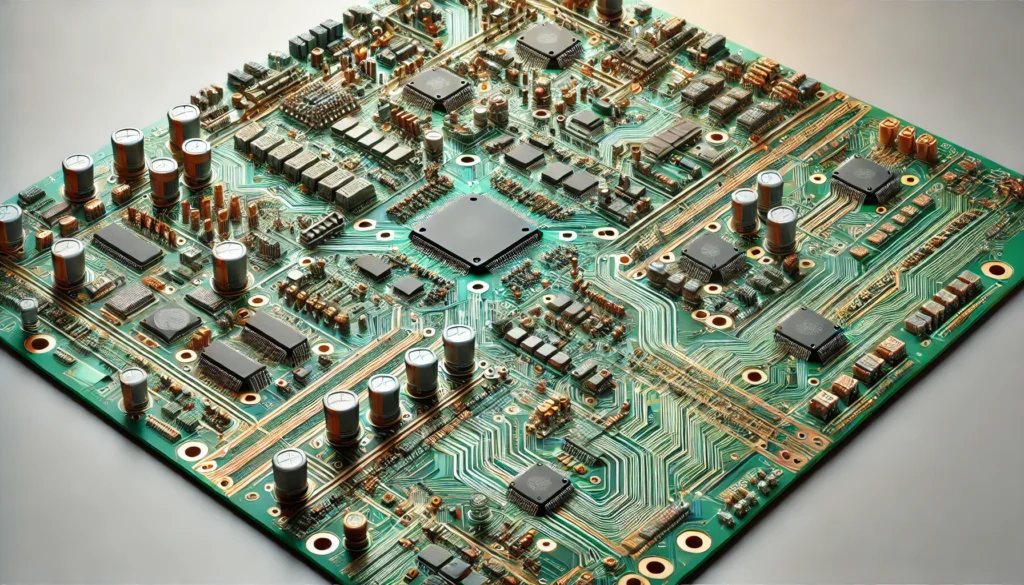
PCB density refers to the number of components and interconnections packed into a given area on a printed circuit board. High-density PCBs allow for more components, often utilising smaller form-factor packages, with tighter routing of connections and traces. This density is critical for modern devices that require high functionality in a compact space, such as smartphones, tablets, and medical devices.
Differences in Standard and High-Density PCB Layouts
While standard PCB layouts typically feature larger components with more space between them, high-density PCBs pack smaller components closer together. Standard PCBs generally have wider traces and fewer layers, while high-density boards require multiple layers and narrower traces to fit everything within a smaller footprint. This compact design approach increases complexity, both in terms of layout and manufacturing.
Component Miniaturisation
One of the driving forces behind high-density PCB design is the miniaturisation of components. Smaller surface-mount devices (SMDs), chip-scale packages (CSPs), and ball grid arrays (BGAs) allow for more components to be placed in a smaller area. This trend toward miniaturisation is critical in meeting the demands for compact, lightweight electronic devices.
Challenges Of High-Density Circuit Board Design
The increasing need for high-density PCBs comes with its own set of challenges. These challenges arise due to the limited space available for routing, the need to maintain power integrity, manage heat dissipation, and ensure signal quality in compact layouts.
Limited Space for Components and Routing
As PCBs become more densely packed, space for routing traces becomes extremely limited. Designers must use multi-layer boards and advanced routing techniques to ensure all components are properly connected without creating signal interference or other issues.
Power Distribution
Power distribution becomes more challenging as the density of components increases. High-density PCBs must accommodate higher current loads while maintaining power integrity across the entire board. Designing efficient power planes and ensuring that decoupling capacitors are placed strategically near sensitive components is critical for avoiding voltage drops and maintaining stable power delivery. Proper power distribution is essential in high-density designs, especially in devices that require consistent power for high-speed data processing, such as smartphones and wearables.
Thermal Management
Managing heat dissipation is critical in high-density designs. Effective heat dissipation strategies must be employed to prevent thermal hotspots, which can degrade performance or even cause component failure. High-power components, such as processors or power regulators, generate significant heat and need to be placed in areas where cooling solutions, such as heat sinks, thermal vias, or active cooling systems, can be applied. Failure to manage heat effectively can lead to reduced reliability and a shorter lifespan for the device.
Signal Integrity Issues
High-density PCBs are particularly prone to signal integrity problems, such as crosstalk and electromagnetic interference (EMI). Maintaining signal integrity in compact layouts requires careful design of trace lengths, controlled impedance, and shielding techniques to prevent performance degradation.
Via and Layer Management
High-density designs often require the use of microvias, blind vias, and buried vias to provide the necessary interconnections between multiple layers. Managing these vias efficiently while balancing manufacturing costs and complexity is a key challenge.
Manufacturing Complexity
Designing a high-density PCB is only the first step; manufacturing these boards also presents significant challenges. The advanced techniques required to produce fine pitch components, high-layer counts, and microvia technology can drive up manufacturing costs and increase the potential for errors.
Component Placement and Shadowing
The placement of components in high-density designs must be precise to avoid shadowing—where one component obstructs access to another. This can complicate soldering, inspection, and repair, making the design and manufacturing process more complex.
Increase in Cost
The advanced materials, manufacturing techniques, and higher complexity involved in designing high-density PCBs typically result in increased production costs. These costs need to be balanced against the performance benefits provided by the compact design.
Best Practices for High-Density PCB Designing
High-density boards require careful attention to every detail, from component selection to routing techniques, in order to ensure that the final product is reliable, efficient, and scalable. By focusing on strategies such as optimising component placement, managing thermal performance, and using advanced routing methods, designers can maximise the performance and longevity of their high-density PCBs.
Component Selection and Placement Strategies
Selecting the right components and placing them strategically is crucial to maintaining signal integrity, managing thermal performance, and ensuring manufacturability. High-density designs require compact, high-performance components that can fit into small spaces without compromising on functionality.
- Choose smaller components like BGAs (Ball Grid Arrays) and CSPs (Chip-Scale Packages).
- Group components by functionality to simplify routing.
- Align components for optimal routing and performance.
- Position heat-generating components strategically for better cooling.
- Ensure adequate clearance and keepout zones for sensitive components.
- Place decoupling capacitors near power pins of critical components.
Smaller footprint components like BGAs and CSPs allow for more connections per square inch, making them ideal for high-density designs. Grouping components by function simplifies routing by keeping related components close, minimising the length of traces, which helps reduce crosstalk and signal degradation.
Efficient orientation of components optimises signal flow, which is especially important for high-speed signals. Components that generate heat should be positioned to facilitate effective cooling, either passively or actively. Additionally, leaving adequate clearance around sensitive components helps with manufacturability and reliability, while decoupling capacitors near power-sensitive components improve power stability and minimise noise.
Routing Techniques
Effective routing ensures that signals are transmitted cleanly without interference, even in compact and complex layouts. This involves leveraging advanced techniques like multi-layer boards, differential pair routing, and proper via management.
- Use multi-layer PCBs for complex designs with limited space.
- Implement differential pair routing for high-speed signals.
- Apply shielding and guarding to reduce electromagnetic interference (EMI).
- Optimise via management with microvias and blind vias for compact inter-layer connections.
- Maintain separate power and ground planes to improve noise reduction and stability.
- Use signal termination techniques to prevent reflections and signal degradation.
Multi-layer PCBs provide the extra space needed for complex designs by separating power, ground, and signal layers, which improves overall signal integrity. Differential pair routing is crucial for high-speed data, as it reduces noise and ensures consistent signal transmission. Shielding and guarding further protect sensitive signals from external noise.
Effective via management, such as using microvias and blind vias, helps reduce space constraints while maintaining proper inter-layer connections. Additionally, separating power and ground planes reduces noise and ensures stable power distribution across the board. Termination techniques, such as adding resistors at trace ends, prevent signal reflections and improve high-speed signal quality.
Conclusion
Designing circuit boards for high-density applications is a complex task that requires careful planning and advanced techniques. By selecting the right components, implementing effective routing strategies, and managing power, signal, and thermal integrity, designers can create high-density PCBs that meet the performance demands of modern devices. The adoption of these strategies is essential for ensuring reliability and cost-effectiveness in today’s rapidly evolving electronics industry.
At Zeus Design, we specialise in creating high-density circuit boards tailored to meet the demands of modern electronics. Our team of experienced engineers uses cutting-edge design techniques to ensure optimal performance, whether you need advanced signal integrity solutions, effective thermal management, or efficient power distribution. We handle the complexities of high-density PCB design, allowing you to focus on bringing innovative products to market.
If you’re looking for a trusted partner in high-density PCB design, explore our PCB Design Services to learn how we can help you achieve success with your next project.
")


0 Comments