
A PCB prototype service gives hardware teams a fast path from verified schematic to functional boards they can test, measure, and iterate on – without committing to a production run. For Australian startups, product companies, and engineering teams, choosing the right pcb prototype service determines how quickly you can close the gap between a design on screen and a validated circuit in your hands. This guide covers what the service actually includes, the decisions that affect turnaround time and quality, and how Zeus Design supports teams through every iteration cycle.
TL;DR
- A PCB prototype service produces small-quantity boards – typically 3 to 20 units – for design validation before committing to a production run.
- Quick-turn fabrication and assembly are distinct steps; coordinating both under one engagement reduces handover risk and compresses lead times.
- Most first-spin PCB prototypes surface at least one layout or component issue – budget for two spins as a baseline.
- Functional testing at the prototype stage, not just visual inspection, is what actually validates a design.
- DFM (Design for Manufacture) decisions made during prototyping cost far less than corrections made after production tooling is committed.
- Zeus Design integrates PCB prototype services with circuit board design, embedded firmware, and DFM review as a single engagement.
Who Uses PCB Prototype Services – and Why
PCB prototyping is not exclusively the domain of hardware startups building a product from scratch. The need for fast, functional boards spans a wide range of engineering situations:
- Hardware startups validating whether their core product idea works on real silicon before raising capital or approaching manufacturers.
- Product teams at established companies adding a connected or sensor-driven PCB to an existing product line.
- R&D engineers testing a new power architecture, wireless protocol, or signal chain before committing it to a production design.
- Industrial OEMs redesigning legacy control electronics to meet modern performance, connectivity, or compliance requirements.
- Inventors and IP holders who need a working demonstration unit for investor presentations, patent applications, or early customer trials.
In each case, the same constraint applies: real learning requires real hardware. Simulation and schematic review can identify many classes of problem, but they cannot replace the information that comes from powering up a physical board, measuring its behaviour with instruments, and running it through its intended operating conditions.
The Australian hardware market adds a practical overlay to this. Component lead times from international distributors, the limited pool of local contract assembly houses, and the coordination overhead of working across time zones with overseas fabricators all create friction that a well-run local PCB prototype service can reduce significantly.
What a PCB Prototype Service Includes
The term “PCB prototype service” is used loosely across the industry. Some providers offer bare-board fabrication only. Others include component procurement and assembly. The most useful engagements – particularly for teams without in-house procurement or assembly capability – cover the full scope from design files to tested boards.
Gerber and Design File Review
Before fabrication begins, the design files – typically Gerber files, drill files, and a bill of materials – go through a computer-aided manufacturing (CAM) review. This checks for manufacturability issues: minimum trace widths and clearances, annular ring sizes, drill-to-copper ratios, and soldermask registration. A rigorous DFM check at this stage catches problems that would otherwise cause fabrication failures or assembly defects.
The IPC-2221 generic PCB design standard defines the baseline tolerances and design rules that fabricators work to. Teams designing PCBs for the first time benefit from understanding which IPC-2221 requirements apply to their layer count and copper weight before submitting for fabrication.
Bare-Board Fabrication
Fabrication converts the PCB design files into a physical laminated board. For prototype quantities, this is typically done on a panel alongside other boards to improve yield and reduce unit cost. Key fabrication parameters that affect lead time and cost include:
- Layer count – 2-layer boards are fastest and cheapest; 4-layer and above add lead time and cost but are often necessary for high-speed digital, RF, or power-sensitive designs.
- Material and Tg rating – Standard FR-4 suits most applications; high-Tg materials are specified for elevated operating temperatures or lead-free assembly processes.
- Controlled impedance – RF, high-speed digital, and USB designs require controlled impedance traces, which adds a fabrication process step and verifying coupon testing.
- Surface finish – HASL (hot air solder levelling), ENIG (electroless nickel immersion gold), and OSP each carry different cost, shelf life, and assembly implications.
Quick-turn fabrication services can deliver 2-layer bare boards in as little as 24 to 48 hours, though Australian-based teams working with overseas fabs need to factor in freight time on top of fabrication lead time. Multi-layer or controlled impedance boards typically run 5 to 10 business days for prototype quantities.
Component Procurement
Component sourcing for a prototype is materially different from production procurement. Prototype quantities are small – sometimes single digits – which means the team is buying at retail or distribution pricing, often across multiple suppliers. The risk at this stage is not cost; it is availability.
Parts specified during schematic capture may be allocated, on long lead time, or already obsolete. A PCB prototype service with component procurement capability will check availability against the BOM before fabrication is ordered, identify substitutes for any at-risk parts, and source through authorised distribution channels to avoid counterfeit exposure. Building BOM alternatives into the design at this stage – before layout is finalised – is significantly cheaper than a PCB respin driven by a component change.
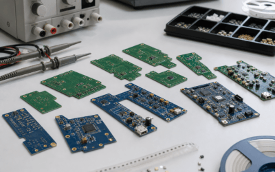
PCB Assembly
Prototype assembly involves placing and soldering components onto the fabricated bare board. For surface-mount components, this is done using solder paste stencils, pick-and-place machines, and reflow ovens even at low volumes – hand soldering prototype boards is increasingly impractical as component sizes shrink. Through-hole components are typically wave-soldered or hand-soldered depending on density and mix.
The IPC-A-610 acceptability standard defines what constitutes an acceptable assembled board – covering solder joint quality, component placement tolerance, and assembly defect classifications. Prototype assemblers working to IPC-A-610 Class 2 or Class 3 provide a meaningful quality baseline that production assemblers will also reference.
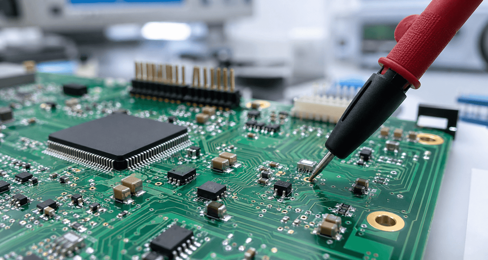
Inspection and Functional Testing
Inspection of assembled prototype boards uses a combination of visual review, automated optical inspection (AOI), and where required, X-ray inspection for hidden solder joints under BGA or QFN packages. AOI catches solder bridges, missing components, and placement errors that are difficult to see with the naked eye at fine-pitch component densities.
Functional testing at the prototype stage is what separates a validated design from an assembled board. This involves powering the board through its intended supply rails, loading firmware, and exercising the core functions against the product specification: measuring signal levels, verifying communication interfaces, testing power consumption at different operating modes, and confirming expected behaviour under edge conditions.
A board that passes AOI but fails functional testing has still taught you something valuable – it has told you where the design needs to change before the next spin. A board that never receives functional testing leaves you with false confidence until later in the programme when problems are more expensive to fix.
When Your Project Needs a Fast-Turn PCB Prototype
Not every prototyping stage calls for a full fabricated PCB. Early in the product development cycle, a proof-of-concept on development boards (STM32 Nucleo, ESP32 devkit, Raspberry Pi Compute Module) validates the core concept at minimal cost. The shift to a fabricated PCB prototype is warranted when:
- The form factor matters – the prototype needs to fit within an enclosure or match a physical interface.
- Component selection requires a custom footprint not available on development boards.
- Signal integrity requirements – RF, high-speed digital, differential pairs – demand a controlled PCB stack-up.
- Power architecture validation requires real power planes and decoupling networks, not breadboard approximations.
- The team is preparing for investor demonstrations or customer trials that require a product-representative unit.
- A DFM review is being planned and needs real boards to assess assembly and test strategy.
The cost of a first PCB spin is not the primary factor in this decision. The primary factor is what technical unknowns remain unresolved and whether they can only be answered by real hardware at the correct layout geometry.
Technical and Commercial Risks to Manage
First-Spin Assumptions
Most first-spin PCB prototypes contain at least one issue that requires a board revision. This is normal and expected – it is not a sign of poor design work. The issues tend to fall into a small number of categories: layout-driven signal integrity problems that simulation did not predict, component pinout errors from an incorrect datasheet interpretation, power supply sequencing issues that only appear under real load, or firmware integration bugs that surface on the actual hardware peripherals.
Planning for two PCB spins from the outset leads to better decisions at every stage. It means the first spin can be optimised for speed and learning rather than trying to over-engineer certainty into an inherently uncertain process. It also means the schedule and budget are realistic rather than optimistic.
Regulatory and EMC Planning
In Australia, electronic products placed on the market are subject to the ACMA regulatory framework, which incorporates Australian/New Zealand EMC and electrical safety standards. Products with intentional wireless transmitters (Wi-Fi, Bluetooth, cellular, LoRa) require ACMA registration. Products connected to mains supply are subject to electrical safety obligations under the relevant state and territory legislation.
The cost of addressing EMC problems discovered during formal compliance testing is orders of magnitude higher than the cost of designing for EMC from the PCB prototype stage. Controlled impedance traces, continuous ground planes, deliberate decoupling placement, and cable/connector earthing strategy are all decisions made during PCB layout – and they are far easier to get right on the first or second PCB spin than to retrofit after the design is otherwise locked.
Component Lifecycle Risk
A component that is readily available at prototype quantities may be on a limited lifecycle or subject to minimum order quantities that are impractical for initial production volumes. The semiconductor supply chain has demonstrated repeatedly that availability assumptions made during prototyping do not always hold at production time. Identifying second-source alternatives at the schematic stage – before layout is committed to a specific footprint – is significantly less disruptive than managing a component substitution after the board is in production.
Firmware and Hardware Integration
Hardware prototyping and firmware development are often treated as sequential – hardware is built first, then firmware is written to run on it. This approach consistently produces the worst outcomes. Firmware that is written against a hardware specification rather than real silicon inevitably encounters interface timing issues, peripheral behaviour differences, and power management interactions that only become apparent on the actual board.
Running firmware development in parallel with hardware design, with firmware tested against development boards until real prototype hardware is available, compresses the validation timeline and surfaces integration issues earlier when they are cheaper to address.
Zeus Design’s PCB Prototype Service
Zeus Design’s rapid prototyping service is built around purposeful iteration rather than a single high-stakes prototype build. The engagement covers the full scope from design files to validated boards, with circuit board design, PCB layout, component sourcing, assembly coordination, and bring-up managed as an integrated programme.
The typical flow for a Zeus Design PCB prototype engagement:
- Design review and requirements confirmation – Zeus Design reviews the product specification, confirms the technology stack and key design parameters, and identifies the specific questions the prototype needs to answer.
- Schematic capture and PCB layout – Full circuit design and PCB layout completed using Altium Designer, with signal integrity, EMC awareness, and DFM considered from the outset. This is delivered by Zeus Design’s circuit board design team rather than treated as a separate handover.
- DFM and design file review – Before fabrication is ordered, the design files are reviewed for manufacturability issues that could affect yield, assembly, or test.
- Component sourcing – Zeus Design manages BOM procurement through authorised distribution, with availability checks and second-source identification for at-risk parts before layout is committed.
- Fabrication and assembly coordination – Zeus Design coordinates with fabricators and assemblers, managing the prototype build programme and tracking the board through fabrication, assembly, and inspection.
- Bring-up and functional validation – Boards are brought up systematically: power rails measured, firmware loaded, core functions validated against the product specification, and any issues documented with root cause analysis to inform the next revision.
- Iteration and next-spin planning – Findings from bring-up are consolidated into a revision plan. Where a second PCB spin is needed, Zeus Design’s layout team turns the revision quickly to maintain programme momentum.
Zeus Design’s embedded software development capability runs in parallel with hardware design throughout this process – ensuring firmware is ready to run on prototype boards as soon as they arrive from assembly, rather than introducing a firmware delay into the validation timeline.
How PCB Prototype Services Connect to Related Capabilities
Circuit Board Design and Layout
The PCB layout is the highest-leverage activity in the prototyping cycle. A well-executed layout reduces EMI, improves signal integrity, simplifies assembly, and sets up the product for a smooth DFM review. Teams that treat layout as a commodity step – separating it from the overall prototyping engagement – routinely generate first-spin issues that could have been avoided with more careful layout practices. Zeus Design’s circuit board design service brings Altium Designer expertise and DFM-aware layout to every prototype, so the board produced during prototyping is a credible predecessor to the production design rather than a throwaway.
Design for Manufacture
DFM is not a post-prototype activity. Decisions about component packaging, pad geometry, panellisation, and test point placement made during the PCB prototype stage are far less expensive to implement than corrections made after the design is otherwise locked. Zeus Design introduces DFM thinking progressively through the prototyping programme – light DFM awareness at the schematic stage, deliberate DFM decisions during layout, and a formal DFM review before committing to a production build. Learn more about Zeus Design’s electronics design service, which includes DFM as a core deliverable.
Full Electronics Design Engagement
For teams who need an end-to-end engineering partner beyond the prototype stage – covering compliance planning, cost optimisation, test jig development, and manufacturing liaison – Zeus Design’s electronics design service extends the prototyping engagement through to production handover. This is particularly relevant for hardware startups planning their first production run, where the transition from prototype to manufacture is where many projects stall. Zeus Design’s published guide on electronics prototyping: turning concepts into hardware covers this transition in more detail.
FAQs
What does a PCB prototype service typically include?
A full PCB prototype service covers design file review, bare-board fabrication, component procurement, PCB assembly, inspection, and functional testing. Some providers offer bare-board fabrication only; others cover the complete scope from Gerber files to tested boards. For teams without in-house procurement or assembly capability, an end-to-end service reduces coordination overhead and compresses the time from design files to validated hardware.
How many PCB prototype spins should I plan for?
Budget for at least two PCB spins for any new design. First-spin prototypes almost always surface layout issues, component behaviour differences, or firmware integration problems that require a board revision. Planning for two spins from the outset leads to more realistic schedules and better first-spin decisions – the first spin can be optimised for speed and learning rather than trying to achieve perfection in a single build.
What is the turnaround time for PCB prototype fabrication in Australia?
Bare-board fabrication for 2-layer prototype PCBs can be completed in 24 to 48 hours at some fabricators, though Australian teams sourcing from overseas fabs need to add freight time. Multi-layer boards with controlled impedance typically run 5 to 10 business days for prototype quantities. Full-service engagements – covering fabrication, component procurement, assembly, and functional testing – typically run 3 to 6 weeks for a first prototype spin depending on BOM complexity and component availability.
What testing should a PCB prototype receive before the next design revision?
At a minimum, prototype boards should receive visual inspection, power rail verification, and functional testing against the product specification before any revision decisions are made. AOI catches assembly defects; functional testing validates that the circuit behaves as designed under real operating conditions. Skipping functional testing and relying on visual or AOI inspection alone is a common cause of problems being discovered later in the programme when they are more expensive to fix.
When should DFM be considered during PCB prototyping?
DFM should be introduced at the PCB prototype stage, not after. Component packaging choices, pad geometry, test point placement, and panellisation decisions made during the first PCB layout are far less expensive to change than post-prototype corrections. A formal DFM review before committing to a production build is strongly recommended regardless of how much DFM attention was applied during prototyping. See Zeus Design’s electronics design service for how DFM is integrated into the full product development lifecycle.
Can Zeus Design manage the full PCB prototype process including assembly and testing?
Yes. Zeus Design’s rapid prototyping service covers the complete scope from design files to tested boards, including schematic design, PCB layout, component sourcing, fabrication coordination, assembly, and bring-up. Firmware development runs in parallel with hardware design so boards are functional as soon as they arrive from assembly, rather than introducing a firmware delay into the validation timeline.
How does a PCB prototype service differ from a production PCB order?
Prototype services are optimised for small quantities – typically 3 to 20 boards – with fast turnaround, design flexibility, and tolerance for iteration. Production orders are optimised for volume, yield, and cost per unit, with higher tooling investment and less tolerance for design changes mid-run. Most products require at least one to two prototype spins before the design is stable enough for a production order, and decisions made during prototyping directly shape production yield and cost.
Taking Your PCB Prototype Forward
Whether you are at first schematic or preparing a prototype for a DFM review, Zeus Design’s team can help you move faster with less risk. PCB prototype services at Zeus Design are designed to produce validated, manufacturable boards – not just assembled units – with circuit board design, firmware, component sourcing, and bring-up managed as an integrated programme rather than a series of disconnected handovers.
If you are planning a prototype build or trying to understand what your next design iteration needs to resolve, the practical guide to PCB design services in Australia covers service scope and partner selection in more detail.
")


0 Comments