
IoT design and development covers every layer of a connected product – from the PCB and embedded firmware on the device, through wireless connectivity, to the cloud backend that stores, processes and serves data. If you are a product owner, founder or engineering manager scoping an IoT build or evaluating a development partner, this guide explains what each layer involves, which decisions must happen early, and where projects most commonly go wrong.
TL;DR
- IoT products span four interdependent layers: hardware, firmware, connectivity and cloud – and decisions made in hardware constrain every layer above it.
- Microcontroller and radio selection must happen early – swapping either mid-project can invalidate months of firmware work.
- Connectivity protocol (Wi-Fi, Bluetooth, cellular, LPWAN) drives PCB antenna design, power budget, firmware stack and cloud architecture.
- Embedded firmware and hardware should be developed in parallel, not sequentially – hardware constraints directly shape what firmware can do.
- Security must be designed in from the hardware layer up, not patched on at the cloud layer.
- A complete IoT product typically also needs a mobile app or web dashboard and a scalable cloud backend – these are not afterthoughts.
- Zeus Design delivers end-to-end IoT products: electronics design, PCB layout, embedded firmware, IoT connectivity, cloud systems and mobile apps under one roof in Australia.

Why IoT Products Are Harder Than They Look
Most connected product failures do not trace back to a single bad decision. They happen because IoT development spans multiple engineering disciplines – electronics, firmware, RF design, cloud infrastructure, mobile – and each layer depends on the others. An MCU selected purely on cost, without checking radio capability, can force a full hardware spin six months into firmware development. A connectivity protocol chosen out of familiarity can blow out the power budget or push antenna design into a regulatory grey zone.
Teams building their first IoT product routinely underestimate this coupling. Software engineers assume hardware behaves like cloud infrastructure – replaceable, patchable, horizontally scalable. Electronics engineers sometimes treat cloud and mobile as someone else’s scope. The result: a product that works in isolation at each layer but fails to integrate, ships late, or needs expensive board respins after the prototype stage.
What follows covers each layer in the order it constrains the rest of the system, explains the key decisions, and flags the risks that most commonly derail IoT projects.
What IoT Design and Development Actually Covers
A complete IoT product has four interconnected layers. Each must be scoped, designed and validated before the product is production-ready.
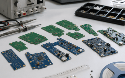
1. Hardware – PCB and Electronics Design
Hardware is the foundation. Every other layer runs on it – and unlike software, hardware changes are expensive once a product reaches prototype or production. Get these decisions right before PCB design begins:
- Microcontroller or microprocessor selection: The MCU choice determines available peripherals, memory, processing headroom, low-power modes and supported radio stacks. Systems-on-chip (SoCs) that integrate radio and processing, such as ESP32 variants, Nordic nRF52 series or Silicon Labs EFR32, simplify BOM and antenna design but may constrain the firmware environment. More capable processors, such as NXP i.MX RT or STM32MP series, offer Linux-capable environments for edge compute but add power, cost and complexity.
- Power architecture: Battery-powered IoT devices require careful power domain design. Selecting between active, sleep and deep-sleep modes, managing inrush current, and selecting regulators that perform well at low-current loads all affect battery life by orders of magnitude.
- Sensor integration: Sensor selection drives interface choices (I2C, SPI, UART, ADC), sampling rate requirements and power consumption. Analog sensor chains require careful PCB layout to avoid noise coupling from switching supplies or RF emissions.
- Antenna design and RF layout: RF is the most underestimated aspect of IoT hardware design. PCB trace antennas require impedance-matched feed lines, ground plane management and keep-out zones. Module-based designs trade layout flexibility for antenna simplicity. Either way, regulatory pre-compliance testing (ACMA in Australia, FCC in the US, CE in Europe) must be planned into the hardware design schedule.
Zeus Design handles the full electronics design process – from schematic capture through multi-layer PCB layout, DFM review and prototype build. Learn more about the end-to-end electronics design service.
2. Embedded Firmware
Firmware runs directly on the IoT device’s microcontroller. It manages hardware peripherals, drives the connectivity stack, handles sensor sampling, implements on-device logic and controls power states. Unlike a web service, firmware runs on constrained hardware – kilobytes of RAM, limited flash, often no operating system, and hard real-time requirements. The architecture decisions made here are difficult to change without a full firmware rewrite.
Key firmware architecture decisions for IoT products:
- RTOS vs bare-metal: Real-time operating systems (FreeRTOS, Zephyr, ThreadX) provide task scheduling, inter-process communication and abstraction layers that simplify complex firmware. Bare-metal development gives finer control over timing and power but becomes difficult to maintain at scale. The right choice depends on processing headroom, timing requirements and team expertise.
- Hardware abstraction layers (HAL): Good firmware separates hardware-specific drivers from application logic. This makes the firmware portable across hardware revisions and dramatically reduces regression risk when the PCB changes.
- Over-the-air (OTA) update capability: Field firmware updates are essential for long-lived IoT deployments. OTA requires dual-bank flash partitioning, a secure bootloader with signature verification, and a rollback mechanism. Designing this in from the start costs far less than retrofitting it after deployment.
- Security primitives: Firmware should implement device identity (unique keys provisioned at manufacturing), mutual TLS or DTLS for cloud communication, and input validation on all external data. According to OWASP’s IoT Security Testing Guide, hardcoded credentials and insecure firmware update mechanisms remain among the most common IoT vulnerabilities.
Zeus Design develops embedded firmware in parallel with hardware, using the same team that designs the PCB. This parallel track – rather than the sequential handoff common at software-only agencies – prevents the late-stage hardware-firmware integration surprises that most often cause schedule blowouts. See the embedded software development service for scope and process.
3. Connectivity – Wireless Protocol Selection
Connectivity protocol is the one decision that flows through everything else – hardware design, firmware complexity, power consumption, regulatory obligations and cloud architecture. Lock this in before PCB layout starts. Changing it after board design begins almost always means a new board spin.
The main protocol categories for IoT products in 2026:
| Protocol | Range | Data rate | Power | Best fit |
|---|---|---|---|---|
| Wi-Fi (802.11b/g/n) | ~50m indoor | High | High | High-bandwidth, mains-powered devices; cameras, gateways |
| Bluetooth Low Energy (BLE) | ~10-100m | Low-medium | Very low | Short-range sensor nodes; wearables; app-connected devices |
| Thread / Zigbee | ~10-100m mesh | Low | Low | Smart home mesh networks; lighting; building automation |
| LoRaWAN | ~2-15km | Very low | Very low | Long-range, low-data sensors; agriculture, utilities, asset tracking |
| LTE-M / NB-IoT | Wide area (cellular) | Low-medium | Low-medium | Mobile or remote devices needing carrier network coverage |
| 5G (sub-6GHz) | Carrier coverage | High | Medium-high | High-bandwidth industrial and edge compute applications |
Hybrid designs – for example, BLE for local device control plus LTE-M for remote data upload – are common but add hardware complexity and certification scope. ACMA spectrum requirements apply to all radio-enabled products sold or operated in Australia, and these must be factored into hardware and firmware design, not treated as a post-design compliance step.
Zeus Design’s IoT connectivity capability covers wireless communication design from protocol selection through antenna layout, RF testing, and cloud-ready data path architecture.
4. Cloud and Backend Architecture
The cloud layer receives, stores, processes and serves data from IoT devices. For most products it also backs the mobile app or web dashboard that users interact with. These cloud architecture decisions must align with device design – not be made independently after the hardware is shipped:
- IoT platform vs custom backend: Managed IoT platforms such as AWS IoT Core or Azure IoT Hub provide device registry, message routing, shadow state and OTA management out of the box. They suit products where cloud infrastructure cost and time-to-market matter more than full control. Custom backends – typically REST or WebSocket APIs backed by time-series databases – offer more flexibility but require more engineering effort and ongoing maintenance.
- Message protocol and serialisation: MQTT is the dominant device-to-cloud protocol for IoT – lightweight, pub/sub, reliable over unstable connections. HTTPS works for infrequent updates but adds overhead. Protocol Buffers or CBOR reduce payload size compared to JSON, which matters on constrained devices and metered cellular connections.
- Data pipeline and storage: IoT products generate time-series data at high volume. Time-series databases (InfluxDB, TimescaleDB, AWS Timestream) handle this workload more efficiently than general-purpose relational databases. Partitioning, retention policies and downsampling should be designed before the product scales to thousands of devices.
- Device management: Production IoT deployments need device provisioning, certificate management, fleet monitoring, remote diagnostics and OTA update orchestration. Designing this in early prevents the operational debt of managing thousands of field devices with no tooling.
Zeus Design builds complete cloud backends for IoT products – device APIs, data pipelines, dashboards and fleet management. The cloud development service is built to integrate directly with the hardware and firmware layers delivered by the same team.
The Mobile App Layer
Most consumer and prosumer IoT products need a companion mobile app for device setup, monitoring, control, notifications and data visualisation. The mobile layer has its own design decisions – and they interact directly with the firmware and cloud layers below it:
- Native vs cross-platform: React Native and Flutter cover the majority of IoT app requirements with a single codebase. Native development (Swift/SwiftUI for iOS, Kotlin for Android) is warranted when BLE throughput, background task timing or platform-specific hardware access is critical.
- BLE pairing and provisioning flows: Device onboarding via Bluetooth is notoriously difficult to get right on all Android variants. Pairing, service discovery, Wi-Fi credential handoff and error recovery require careful handling – and testing on a wide range of physical devices, not just emulators.
- Real-time data display: Apps polling a cloud API every 5 seconds will drain battery and add latency. WebSocket connections or push notification architectures provide lower-latency device state updates for time-sensitive monitoring applications.
Zeus Design’s mobile app development service covers iOS, Android and cross-platform apps with direct integration to IoT hardware and cloud backends. The same team that builds the cloud backend also builds the app, which eliminates the API contract disputes that are common when mobile and backend are developed separately.
Technical and Commercial Risks in IoT Projects
IoT products fail more often than pure software products because hardware mistakes are expensive to fix post-manufacture. These are the risks that most frequently derail projects:
Protocol lock-in
Selecting a connectivity protocol based on what a developer knows rather than what the application requires is the most common source of expensive hardware respins. Protocol selection drives PCB layout, antenna design, firmware stack, certification scope and cloud architecture. Changing the protocol after PCB design is started typically means a new board spin.
Power budget overrun
Battery-life claims made at the architecture stage rarely survive contact with real firmware. Interrupt latency, unexpected peripheral wakeups, radio retry storms and poor sleep state management all erode battery life. Power profiling at the firmware level, using tools such as the Nordic PPK2 or Segger J-Trace, should happen before hardware is finalised.
Regulatory compliance left too late
In Australia, radio devices must comply with ACMA requirements under the Radiocommunications Act. CE and FCC marks are required for international markets. Pre-compliance testing on prototype hardware – checking conducted and radiated emissions before the formal certification test – catches layout and firmware issues before they become expensive last-minute redesigns. This is covered under Zeus Design’s electronics design and compliance service.
Security as an afterthought
IoT security failures consistently trace back to decisions made at the hardware or firmware layer – hardcoded keys, unsigned firmware, no device identity, unencrypted communications. Retrofitting security onto a shipped product is expensive and often incomplete. The ETSI EN 303 645 standard provides a practical baseline for consumer IoT security requirements.
Underestimating production readiness
A working prototype is not a production-ready design. DFM review, test coverage, manufacturing documentation, programming jig design and supply chain validation all add scope between prototype and first production run. Teams that scope only to “working prototype” frequently find themselves with a second major project phase that was not budgeted.
Zeus Design’s IoT Development Process
Zeus Design takes IoT products from brief to build as a single integrated team. The process typically runs as follows:
- Discovery and architecture: Define the product requirements, connectivity constraints, power budget, regulatory obligations and cloud data model before any design work begins. Block-diagram the full system across hardware, firmware, connectivity and cloud.
- Hardware design: Schematic capture, component selection, PCB layout, DFM review and pre-compliance RF planning. Parallel firmware environment setup and HAL skeleton development.
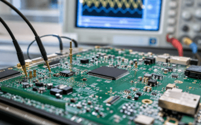
- Prototype build and bring-up: PCB fabrication and assembly, hardware bring-up, peripheral driver development and initial firmware integration testing. Power profiling and RF characterisation on real hardware.
- Firmware and cloud development: Full firmware stack – sensor drivers, connectivity stack, application logic, OTA update system and security provisioning. Cloud backend – device API, message pipeline, storage and device management. Mobile app – onboarding, monitoring, control and notification flows.
- Integration and validation: End-to-end system testing across hardware, firmware, cloud and mobile. Security review. Pre-compliance RF and emissions testing.
- Production readiness: DFM sign-off, manufacturing documentation, test jig development and supply chain validation. Handover to manufacturing partner.
This integrated approach – one team across electronics, firmware, cloud and mobile – removes the handoff gaps that most commonly cause IoT projects to run over time and budget.
How IoT Connects to Related Services
IoT design and development rarely stands alone. Most IoT products draw on several Zeus Design capabilities in parallel:
- Electronics Design: Hardware architecture, schematic, PCB layout, DFM and compliance planning.
- Embedded Software Development: Firmware for microcontrollers and connected hardware, developed alongside electronics.
- Cloud Development: Device APIs, IoT backends, data pipelines and fleet management systems.
- Mobile App Development: Companion apps for iOS and Android with hardware and cloud integration.
- Rapid Prototyping: Quick-turn proof-of-concept builds to validate hardware feasibility before full design investment.
For teams that have already completed prior IoT posts, the IoT Development: Hardware, Firmware and Cloud in 2026 post covers the development lifecycle in further depth, and IoT Design Services: From Hardware to Cloud in 2026 covers service selection criteria.
FAQs
What does IoT design and development include?
IoT design and development covers the full stack of a connected product: electronics hardware and PCB design, embedded firmware, wireless connectivity, cloud backend infrastructure, and often a mobile or web app. A complete IoT product requires all these layers to be designed to work together – each layer has hard dependencies on the others, so they cannot be treated as independent workstreams.
How long does it take to develop an IoT product from scratch?
A complete IoT product – hardware, firmware, cloud and mobile – typically takes 9 to 18 months from architecture to production-ready, depending on complexity, connectivity requirements and regulatory obligations. Simple sensor products with existing reference hardware can move faster. Products requiring custom RF design, multi-protocol connectivity or complex cloud infrastructure take longer. Cutting the prototype phase short to save time nearly always costs more time at the integration and compliance stages.
What wireless protocol should I use for my IoT product?
The right protocol depends on range, data rate, power budget, infrastructure availability and regulatory obligations. BLE suits short-range, battery-powered, app-connected devices. LoRaWAN suits long-range, low-data, outdoor sensor applications. LTE-M or NB-IoT suits mobile or remote devices that need carrier coverage. Wi-Fi suits high-bandwidth, mains-powered devices. A Zeus Design architecture review will define the right protocol before PCB design begins – see the IoT connectivity service for more detail.
Can a software development agency build an IoT product?
Software-only agencies can build the cloud and mobile layers, but they cannot design hardware, lay out PCBs, develop embedded firmware or manage RF compliance. IoT products require electronics engineering capability alongside software development. Splitting hardware and software across separate agencies creates integration risk – protocol contracts, timing assumptions and security provisioning must be agreed in detail, and gaps between teams are where most IoT project failures originate.
What are the most common IoT development mistakes?
The most common mistakes are: selecting a connectivity protocol without fully understanding the power, range and regulatory implications; treating firmware as an afterthought rather than developing it in parallel with hardware; leaving security design until after the prototype is working; underestimating the scope gap between a working prototype and a production-ready design; and failing to plan OTA firmware update capability before deployment.
How much does IoT product development cost in Australia?
Cost varies significantly with product complexity, connectivity requirements, regulatory scope and the number of software layers needed. A simple sensor product with BLE and a basic mobile app may be in the AUD $80,000-$150,000 range for a first prototype. A product with custom RF design, multi-protocol connectivity, a full cloud backend and iOS/Android apps will typically be in the AUD $200,000-$500,000+ range. Zeus Design provides scoped estimates after an architecture review – contact the team to discuss your project.
Does Zeus Design handle IoT compliance and certification?
Yes. Hardware compliance planning – pre-compliance RF testing, EMC layout review, ACMA (Australia), FCC (US) and CE (Europe) documentation – is part of Zeus Design’s electronics design process. Compliance is planned into the hardware design from the start, not treated as a post-design test. This approach significantly reduces the risk and cost of formal certification failures.
Conclusion
Building an IoT product well means designing all four layers – hardware, firmware, connectivity and cloud – as a single system, not handing them off sequentially between teams. The decisions made at the hardware layer constrain everything above it, and by the time those constraints become visible to a software team, the cost to fix them has already compounded.
Zeus Design delivers complete IoT products – electronics design and PCB layout through embedded firmware, IoT connectivity, cloud backends and mobile apps – as a single integrated team in Australia. If you are scoping an IoT product or need an honest assessment of whether your existing design is production-ready, start with an architecture conversation.
")
0 Comments