
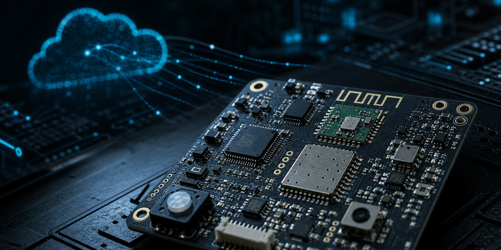
An IoT design service should cover far more than writing firmware or picking a wireless module – it spans hardware architecture, connectivity selection, embedded software, cloud integration and production handover. This guide is for product teams, startup founders and engineering managers evaluating what a specialist IoT partner should actually deliver, and how Zeus Design’s electronics design and IoT connectivity services address each layer of that stack.
TL;DR
- A complete IoT design service covers hardware architecture, PCB design, wireless connectivity, firmware, cloud backend, mobile or web interface, and production handover.
- Connectivity choice – Wi-Fi, Bluetooth, cellular, LoRaWAN or Zigbee – must be resolved early because it drives PCB layout, antenna design, power budget and cloud architecture.
- Firmware and cloud must be designed together. Misaligned data formats, OTA update strategies or security models cause expensive rework after integration.
- Compliance (FCC/CE/RCM) and design for manufacture should be considered from the first schematic, not treated as a final-stage checklist.
- Zeus Design delivers IoT products across the full stack – from electronics design and PCB layout through firmware, cloud systems and mobile apps.
Why IoT Product Teams Struggle to Find the Right Partner
Most hardware startups and product teams face the same structural problem: IoT products require competence across at least four distinct engineering disciplines – electronics hardware, embedded firmware, cloud systems and user-facing software. Few internal teams hold all four. Outsourcing to specialists in only one layer usually creates handover friction, integration failures and timeline blowouts.
The typical failure mode looks like this: a team hires a firmware contractor who delivers embedded code that assumes a cloud data model that was never defined. Or a PCB designer produces a board with a Wi-Fi module that draws too much current for the battery life the product needs. Or compliance testing fails because antenna placement was optimised for layout convenience rather than RF performance.
These are not edge cases – they are predictable consequences of treating IoT as a collection of separable services rather than a tightly coupled system. A quality IoT design service treats the hardware, firmware and cloud as a single system and designs them together.
This guide explains what each layer of that system should include, what decisions need to be made early, and what a specialist partner should be accountable for delivering.
What an IoT Design Service Should Include
1. Hardware Architecture and Electronics Design
The first deliverable from any IoT engagement is a hardware architecture document – a clear description of the compute platform, sensor suite, connectivity stack, power system, and mechanical constraints. This is not a marketing slide deck; it is an engineering specification that drives every downstream decision.
Hardware architecture for IoT differs from standard electronics design in several important ways. Power budget is a first-class design constraint from the start – whether the device runs on mains power, a rechargeable battery or primary cells changes microcontroller selection, wireless protocol choice and PCB topology. Sensor integration adds analogue complexity that many purely digital teams underestimate. And connectivity hardware – antennas, RF front ends, modem modules – introduces regulatory and RF design requirements that affect board layout from layer 1 onward.
A specialist should be comfortable designing around common IoT compute platforms (ESP32, STM32, nRF52 series, i.MX RT and similar families), selecting appropriate sensor ICs, and producing a schematic that can survive a production DFM review. Zeus Design’s electronics design service covers this complete hardware architecture phase, from component selection through to production-ready schematics and PCB layout.
2. PCB Design and Layout for Connected Devices
IoT PCBs carry a specific set of layout challenges that general-purpose PCB design work does not always address. RF traces, antenna keep-out zones, impedance-controlled differential pairs for high-speed interfaces, and current path management for devices that switch between sleep and active modes are all standard requirements.
A wireless module placed incorrectly relative to power planes, ground pours or board edge will fail RF certification regardless of how well the firmware performs. Antenna placement and ground plane management must be treated as first-order layout constraints, not aesthetic choices. Authoritative guidelines from module manufacturers – for example Espressif’s hardware design guidelines or Nordic Semiconductor’s antenna tuning notes – define clear keep-out and ground-pour rules that a competent IoT layout engineer will follow.
Zeus Design’s circuit board design service handles multilayer IoT PCBs with impedance control, RF-aware layout, and DFM checks aligned to production assembly requirements.
3. Wireless Connectivity Selection
Connectivity is the decision with the longest tail of consequences. The right choice depends on range, data rate, power budget, network topology, infrastructure requirements and target markets. Getting it wrong late in a project is expensive – it typically means a board respin and a firmware rewrite.
The main options and their trade-offs:
- Wi-Fi (802.11 b/g/n/ac): High data rates, short range, high power draw in transmit mode. Best for mains-powered devices with high data throughput requirements such as cameras, industrial gateways and appliances. Relies on existing network infrastructure.
- Bluetooth Low Energy (BLE): Low power, short range (typically 10-30 m), suitable for wearables, asset trackers and devices that sync to a nearby smartphone. The Bluetooth SIG maintains the core specification and profile documentation.
- Cellular (LTE-M / NB-IoT / Cat-1): Long range, wide area coverage without local infrastructure, moderate power. Best for field devices, remote monitoring, fleet tracking. Requires SIM management and carrier agreements.
- LoRaWAN: Very long range (2-15 km), very low power, low data rate. Best for battery-powered sensors reporting infrequently over wide areas – agriculture, utilities, environmental monitoring. Requires gateway infrastructure or The Things Network coverage.
- Zigbee / Thread / Matter: Mesh networking, low power, short range. Best for smart home and building automation scenarios where devices form a local mesh rather than connecting to the internet directly.
A well-scoped IoT design service will run a connectivity selection review before schematic work begins. This is not a bullet-point comparison – it requires calculating the actual power budget at the system level, validating coverage assumptions against deployment environment data, and confirming that the chosen stack has a path to regulatory certification in your target markets.
4. Firmware and Embedded Software Development
Firmware for an IoT device is not a simple embedded application. It must manage hardware peripherals, implement wireless protocols, handle secure connectivity to cloud infrastructure, manage power states, support OTA (over-the-air) updates, and do all of this on a resource-constrained platform with limited RAM and flash.
A quality IoT firmware engagement should deliver:
- Hardware abstraction layers (HALs) and peripheral drivers for all onboard sensors and interfaces.
- RTOS integration or bare-metal task scheduling appropriate to the application complexity.
- Wireless protocol stack integration – Wi-Fi provisioning, BLE GATT profiles, LTE-M/NB-IoT modem management, or LoRaWAN MAC layer integration.
- Secure TLS/DTLS transport for cloud communication, with certificate management and key storage appropriate to the hardware security capabilities (secure element, TrustZone, or software-only approaches).
- OTA firmware update capability with rollback protection.
- Power management – sleep modes, wake-on-interrupt, radio duty cycling.
- Watchdog, fault logging and recovery mechanisms for unattended field deployment.
Zeus Design develops firmware alongside hardware – the same team that specifies the schematic writes the embedded software. This avoids the integration friction that occurs when firmware contractors work from a completed board they did not influence. The embedded software development service covers the full firmware stack from peripheral drivers through to cloud connectivity and OTA update infrastructure.
5. Cloud Integration and Backend Architecture
The cloud layer is where most IoT projects run into architectural debt. Data models defined informally during firmware development become rigid constraints that are expensive to change once devices are deployed in the field. Security posture decided as a prototype shortcut becomes a liability when the product reaches production.
A specialist IoT design service should define the cloud architecture before firmware work begins, not after. Key deliverables include:
- Device registry and fleet management architecture – how devices are provisioned, authenticated and managed at scale.
- Telemetry ingestion pipeline – MQTT broker or HTTP endpoint, message routing, data normalisation, time-series storage.
- OTA update infrastructure – update package signing, staged rollout, version tracking, rollback triggering.
- API layer – REST or GraphQL endpoints that mobile apps and web dashboards consume.
- Alerting, anomaly detection and operational monitoring.
- Security model – mutual TLS, device certificates, API key management, data encryption at rest and in transit.
AWS IoT Core, Azure IoT Hub and Google Cloud IoT are the dominant managed platforms. Each has official documentation covering device provisioning, security best practices and fleet management that a competent cloud architect will follow rather than reinvent. Zeus Design’s cloud development service handles IoT backend systems built on these managed platforms, designed to scale from prototype fleet to production volume without architectural rework.
6. Mobile App and Dashboard Development
Most IoT products require a user-facing interface – either a mobile app for consumer and prosumer devices, or a web dashboard for industrial and commercial applications. This layer is often scoped separately but is tightly coupled to the firmware data model and cloud API.
A mobile app for an IoT product is not a standard CRUD application. It needs Bluetooth or Wi-Fi provisioning flows for device onboarding, real-time data streaming from cloud websockets or push notifications, BLE communication for local control, and offline behaviour when connectivity is intermittent. Zeus Design’s mobile app development service handles iOS, Android and cross-platform development for IoT-connected products, including BLE and Wi-Fi provisioning, cloud integration and automated testing.
7. Compliance and Regulatory Planning
Wireless IoT devices sold in Australia require RCM (Regulatory Compliance Mark) certification. Devices sold in the US require FCC authorisation; EU devices require CE marking. Each of these involves radio frequency testing, conducted emissions testing, and for some product categories, safety testing.
Compliance is not a bolt-on activity. PCB layout decisions – antenna placement, shielding, ground plane management – directly affect emissions test results. A design that ignores compliance planning until pre-certification testing typically requires one or more board respins. The Australian Communications and Media Authority (ACMA) publishes the technical standards and labelling requirements that apply to wireless devices supplied in Australia.
A specialist IoT design service will maintain compliance awareness from the first hardware architecture review – selecting pre-certified modules where appropriate, designing board keep-outs to module vendor specifications, and flagging custom antenna designs that will require full certification testing.
8. Design for Manufacture and Production Handover
A successful prototype is not a production-ready product. Design for manufacture (DFM) for IoT devices addresses component standardisation, assembly panelisation, test jig design, and BOM management for supply chain risk. Production test coverage – verifying wireless connectivity, sensor calibration and firmware integrity on every unit – requires dedicated test infrastructure that must be designed alongside the product.
Zeus Design includes DFM review and test jig development as part of the electronics design engagement, ensuring that the path from validated prototype to volume production is planned rather than improvised.
When Does a Project Need a Full-Stack IoT Design Service?
Not every IoT project needs a partner who covers all eight layers above. A team with strong firmware capability might only need hardware design and cloud architecture support. A team with cloud infrastructure experience might need hardware, firmware and mobile app delivery.
The clearest case for a full-stack IoT design service is when:
- The internal team holds fewer than two of the required disciplines in depth.
- The product requires custom hardware – not an off-the-shelf development kit or reference design adapted to a new enclosure.
- The target market requires wireless certification and the team has not run a certification programme before.
- The project timeline cannot absorb integration delays caused by handover between separate contractors.
- The device will be deployed in the field in large numbers, making OTA update infrastructure, fleet management and production test coverage critical from the start.
Technical and Commercial Risks to Manage
IoT projects carry a specific set of risks that differ from pure software projects or standard electronics design work. The most common ones are:
- Connectivity integration failure: Firmware and cloud data models defined independently without a shared contract. Results in integration delays and field reliability problems.
- Power budget overruns: Battery life projections based on datasheet figures rather than measured system behaviour. Common when hardware and firmware are developed separately.
- RF certification failure: Board layout not reviewed against module vendor RF guidelines. Typically discovered at pre-compliance testing, requiring a board respin.
- Security model debt: Prototype shortcuts – hardcoded credentials, no certificate rotation, plain HTTP – carried forward into production.
- OTA update gaps: No rollback mechanism for failed updates on field-deployed devices. A single bad firmware release can brick the entire fleet.
- Production test gaps: No automated test coverage for wireless connectivity at production. Boards with failed antennas or misconfigured modems ship to customers.
Zeus Design’s IoT Process and Deliverables
Zeus Design approaches IoT product development as a single integrated engagement rather than a collection of separate service contracts. The process runs in overlapping phases:
- Discovery and architecture: Hardware architecture, connectivity selection, cloud architecture, security model, compliance strategy and project phasing. Output: architecture specification and project plan.
- Hardware design: Schematic design, BOM selection, PCB layout with RF-aware routing, DFM review. Output: production-intent Gerber files and BOM.
- Firmware and cloud development: Peripheral drivers, protocol stack integration, cloud connector, OTA infrastructure, device provisioning. Developed in parallel with hardware iteration.
- Integration and validation: End-to-end system testing, power measurement, RF pre-compliance checks, security review. Output: validated prototype and test report.
- Production readiness: Test jig development, production firmware configuration, compliance submission support, manufacturing documentation package.
This structure ensures that firmware and cloud work begin before the PCB is finalised – reducing calendar time and catching integration assumptions early when they are cheap to resolve.
How IoT Design Connects to Related Services
IoT product development draws on most of Zeus Design’s core service areas. Electronics design and PCB layout provide the hardware foundation. Embedded software development covers firmware and protocol stacks. Cloud development handles the backend infrastructure. Mobile app development delivers the user-facing interface. And rapid prototyping enables early validation of hardware assumptions before full design investment.
For teams that need to move quickly from concept to a working prototype, Zeus Design’s rapid prototyping service can produce a functional proof-of-concept board within weeks – enough to validate connectivity, power budget and sensor integration before committing to a production PCB design.
FAQs
What does an IoT design service actually include?
A complete IoT design service covers hardware architecture, PCB design, wireless connectivity integration, firmware and embedded software, cloud backend, user interface (mobile app or web dashboard), compliance planning and production handover. Most engagements cover all of these layers to avoid handover problems between separate contractors. Zeus Design’s electronics design service covers the hardware and firmware layers as part of a single integrated engagement.
How early should I engage an IoT design partner?
As early as possible – ideally before any hardware is selected. Connectivity choice, power architecture and cloud data model decisions made in the first two weeks of a project have downstream consequences for PCB layout, firmware architecture, certification cost and production test design. Engaging a specialist after a prototype already exists usually means inheriting architectural decisions that are expensive to revisit.
What wireless protocol is best for IoT products?
There is no single best protocol. Wi-Fi suits high-throughput mains-powered devices. Bluetooth Low Energy suits battery-powered devices that pair to a smartphone. Cellular (LTE-M or NB-IoT) suits field-deployed devices without local infrastructure. LoRaWAN suits low-power sensors reporting infrequently over wide areas. The right choice depends on power budget, range, data rate, deployment environment and certification requirements – a connectivity selection review should always precede hardware selection.
Do IoT devices need wireless certification in Australia?
Yes. Wireless transmitters sold or supplied in Australia must carry the RCM mark, which requires compliance with the Australian Communications and Media Authority’s (ACMA) technical standards for radiocommunications equipment. Devices also sold in the US or EU require FCC authorisation or CE marking respectively. Compliance planning should start at hardware architecture, not at pre-production testing, to avoid board respins.
What is OTA firmware update infrastructure and why does it matter?
OTA (over-the-air) update infrastructure is the system that allows firmware on deployed devices to be updated remotely without physical access. It matters because field-deployed IoT devices accumulate security vulnerabilities, protocol changes and bug fixes over their lifetime. Without a robust OTA system – including update signing, staged rollout and rollback protection – a single bad firmware release can render deployed units inoperable and require costly physical servicing.
Can Zeus Design deliver only part of the IoT stack?
Yes. While full-stack engagement is often the most efficient approach, Zeus Design can deliver specific layers – hardware design only, firmware only, cloud backend only, or mobile app only – for teams that have existing capability in some areas. The key requirement is a clear API contract and data model agreement at the layer boundaries before work begins, to avoid integration problems downstream.
How long does an IoT product development project take?
A first working prototype for a custom IoT device typically takes 3-6 months from architecture to validated hardware, depending on complexity. Production-ready status – including DFM review, compliance testing and production test infrastructure – typically adds 2-4 months beyond that. Timelines compress significantly when firmware and cloud development run in parallel with hardware iteration rather than sequentially after the first PCB is built.
Conclusion
An IoT design service is only as strong as its weakest layer. Hardware built without firmware input produces integration problems. Firmware written without a defined cloud data model produces expensive rework. Connectivity selected without a power budget analysis produces field failures. Compliance planning deferred to the end of the project produces board respins.
The engineering discipline required to avoid these outcomes is not mysterious – it is systematic integration of hardware, firmware, cloud and compliance thinking from the first architecture decision. That is what distinguishes a specialist IoT design service from a collection of contractors working in sequence.
Zeus Design delivers IoT products across the full stack – electronics design, PCB layout, embedded firmware, cloud backend and mobile apps – from a single team that understands how each layer constrains the others. If you are scoping an IoT product or evaluating whether your current development approach is set up to succeed, the most useful first step is a structured architecture conversation.
See also: IoT Development: Hardware, Firmware and Cloud in 2026 and IoT Design Services: From Hardware to Cloud in 2026 for further context on how Zeus Design approaches connected-device projects.
")


0 Comments