An electronic prototyping service takes a product concept and turns it into a functional, testable circuit board – one your team can evaluate, iterate, and prepare for manufacture. This guide is written for hardware startup founders, product managers, and engineering teams evaluating prototyping partners or planning a first prototype build. It covers the process from schematic capture to assembled board, with practical guidance on iteration cycles, DFM readiness, and what a production-minded approach actually involves.
TL;DR
- Electronic prototyping turns a schematic into a physically assembled, testable PCB – usually across 2-4 iteration cycles before a design is production-ready.
- A quality prototyping service covers circuit design, PCB layout, component sourcing, assembly, firmware bringup, and functional testing – not just bare board fabrication.
- DFM (Design for Manufacture) considerations belong in the prototype stage, not after it. Retrofitting manufacturability is expensive and slow.
- Iteration cycles are normal and expected. The goal is to fail fast and cheaply on the bench, not in production.
- Choosing an integrated partner – one who handles hardware and firmware together – reduces interface risk between disciplines.
- Zeus Design offers rapid electronics prototyping in Australia with a 2-8 week turnaround, full IP transfer, and a DFM-ready handover process.
Context and Audience
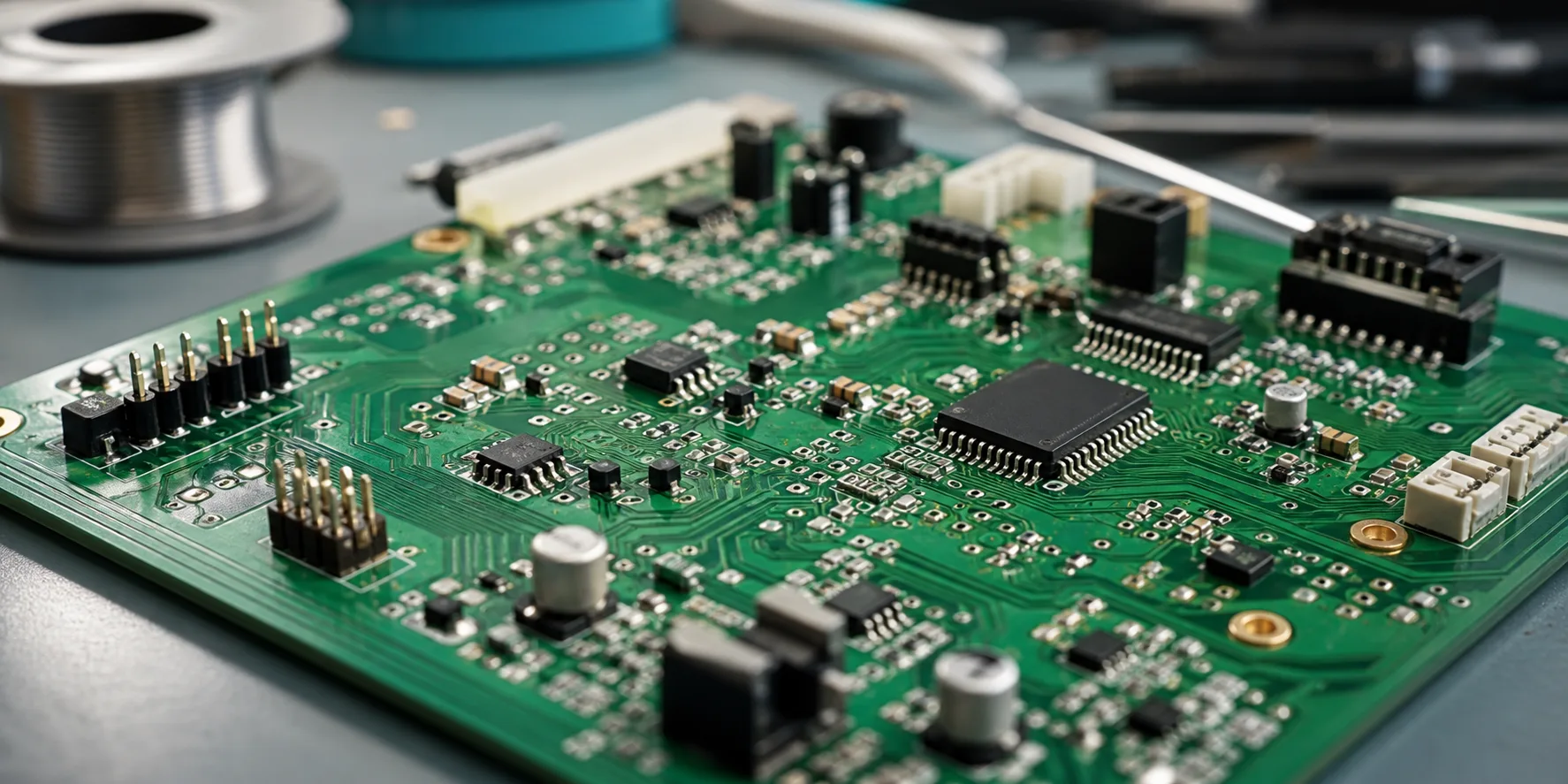
Most hardware products fail not because the concept was wrong, but because the team moved too slowly through early validation or skipped essential engineering steps under time pressure. The result is a prototype that looks functional in isolation but falls apart under real-world conditions – or a design that works on the bench but cannot be assembled at volume without significant rework.
Electronic prototyping services reduce that risk. A specialist partner brings circuit design experience, PCB layout tools, component libraries, and assembly capability under one roof – allowing a product team to move from a requirements brief to a working board in weeks rather than months.
This guide is relevant if you are:
- A startup founder with a hardware concept and no in-house electronics engineering capacity.
- A product manager at an established company needing a functional proof-of-concept before committing to in-house development.
- An engineering team that designs electronics internally but wants a faster or more structured prototyping process for a new product line.
- An inventor or industrial business evaluating whether a concept is feasible before investing in a full design engagement.
What an Electronic Prototyping Service Includes
The term “prototyping” is used loosely across the industry. Some services provide bare board fabrication only – you supply the Gerber files, they manufacture the PCB, and assembly is your problem. Others offer a full-service engagement covering everything from circuit design through to a tested, documented board ready for iteration.
A full-service electronic prototyping service typically covers:
- Requirements capture – defining functional requirements, operating conditions, power budget, connectivity needs, and regulatory targets before any design work begins.
- Schematic design – capturing the circuit topology in an ECAD tool (Altium Designer is the industry standard for professional-grade work), including component selection, signal path planning, and power architecture.
- PCB layout – translating the schematic into a routed, layered board with appropriate trace widths, impedance control, component placement, and design rule compliance.
- Gerber file generation and fabrication submission – producing standardised manufacturing outputs (Gerbers, BOM, pick-and-place files, NC drill files) and submitting them to a PCB fabricator with any relevant DFM notes.
- Component sourcing – procuring components from authorised distributors, managing lead times, and handling substitutions where necessary.
- PCB assembly – soldering components to the board, either manually (for low-complexity or through-hole boards) or via SMT reflow and automated assembly.
- Firmware bringup – loading embedded software, initialising peripherals, and confirming basic hardware functionality at power-on.
- Functional testing – verifying that the board performs as specified, identifying failures, and feeding results back into the next design iteration.
- Documentation – schematics, BOM, PCB layout files, test results, and design notes that support the next iteration or production handover.
The right scope depends on where your design sits today. Some engagements start from a rough block diagram; others hand over a near-complete schematic and need layout, assembly, and testing only.
When a Project Needs a Prototyping Service
Not every project is at the right stage for formal electronics prototyping. Some concepts still need feasibility analysis or a proof-of-concept before committing to a full PCB design. Others are ready to move directly into prototype and iterate from there.
A prototyping service is the right engagement when:
- The concept has been validated at a high level (a block diagram exists, the core technical approach is defined) and the team is ready to build something that can be tested with real electronics.
- The design needs to demonstrate specific performance characteristics – power consumption, RF range, sensor accuracy, response time – that cannot be confirmed without physical hardware.
- Regulatory or compliance requirements (CE, FCC, RCM in Australia) need to be identified early so the design can account for them from the start.
- The product will eventually go to volume manufacture, and the team wants to begin building DFM knowledge into the design rather than retroactively fixing it.
- Investment or commercialisation decisions depend on a working demonstration of the technology.
If the concept has not yet been technically defined, a proof-of-concept build may be the better starting point – a faster, lower-cost build that answers a specific feasibility question before the full prototyping cycle begins.
The Iteration Cycle: From Schematic to Working Board
A common misconception in hardware product development is that the goal is to get the first prototype right. The more productive mental model is that each prototype is a structured experiment designed to answer specific questions and surface specific failure modes. The goal is to fail fast and cheaply on the bench.
The most productive way to run an electronics prototype is to treat each build as a controlled experiment with defined pass/fail criteria – not as an attempt to produce a finished product. Teams that adopt this discipline consistently converge to a production-ready design faster than those chasing perfection in every iteration.
A typical iteration cycle runs as follows:
- Define test objectives for this iteration – what specific questions does this build need to answer? What failure modes are you trying to surface? What minimum performance targets does the board need to hit?
- Update schematic and layout – incorporate findings from the previous iteration (or start from the initial design), complete the schematic capture, and run DRC (design rule check) before proceeding to layout.
- Review before fabrication – a pre-fabrication review catches layout errors, netlist mismatches, and DFM issues before PCBs are manufactured. This is significantly cheaper than discovering problems after assembly.
- Fabricate, source components, assemble – quick-turn PCB fabrication services can deliver bare boards in 24-72 hours for standard stackups. Assembly follows, either manually or via SMT pick-and-place.
- Bringup and test – power-on, firmware load, peripheral initialisation, and systematic functional testing against the objectives defined in step one.
- Document findings – what worked, what failed, what needs to change, and what the next iteration needs to prove. This documentation drives the next cycle.
Most hardware products require 2-4 prototype iterations before the design is ready for DFM review and production handover. Complex products – those with RF subsystems, high-speed digital interfaces, or tight power budgets – often need more. Plan the budget and timeline for multiple iterations from the start. The most common and costly mistake in early-stage hardware is treating the first prototype as a final design.
For more on how prototyping fits into the wider electronics development process, see our guide to electronics prototyping: turning concepts into hardware.
DFM Readiness – Building With Production in Mind
Design for Manufacture (DFM) is one of the most underweighted considerations in early-stage hardware prototyping. Teams optimise for getting a working board quickly – which is correct – but often make design choices during prototyping that create significant cost and schedule problems at production.
DFM-aware prototyping does not mean designing for mass production from day one. It means making choices during prototyping that do not actively block a clean production transition later. Key DFM considerations to address during the prototyping phase include:
- Component selection – specifying components available in production-relevant quantities from authorised distributors, and avoiding single-source parts where alternatives exist.
- Package choice – using component packages compatible with standard SMT assembly processes. Exotic or very fine-pitch packages increase assembly cost and defect rate at volume.
- Panelisation-ready layout – PCB dimensions and board edge clearances that allow panels to be created for volume assembly without layout redesign.
- Test point placement – including physical test points on the PCB for functional test access during production. Retrofitting test access after production tooling is in place is expensive.
- Compliance pre-checks – early-stage EMC layout practices (ground plane integrity, high-frequency trace routing, decoupling capacitor placement) that reduce certification risk later. The IPC standards body publishes widely-used PCB design and assembly standards (IPC-2221, IPC-A-610) that define acceptable manufacturing thresholds for production boards.
According to Altium’s prototyping documentation, PCB prototyping services use standard stackups and production-level assembly processes – meaning the prototype fabrication and assembly workflow directly reflects what volume manufacture will look like. Teams that treat prototyping as a separate world from production lose this alignment.
Zeus Design’s electronics design service incorporates DFM review throughout the prototyping cycle, not only at the production handover stage.
Technical and Commercial Risks to Manage
Electronic prototyping involves predictable risks that good project management and the right partner can address proactively.
Component availability and lead times
The global semiconductor supply chain remains volatile. Components specified during prototype design may have 20-52 week lead times at production volumes, or may be discontinued by the time the product reaches market. Digi-Key’s supply chain resources are a practical reference for checking real-time component availability and lead times during the design phase. A prototyping partner with active distributor relationships and broad component library access can identify availability risk early and propose alternatives before the design is locked.
Schematic-to-layout translation errors
Errors introduced during PCB layout – reversed component polarity, missing vias, incorrect footprints, signal integrity violations – are common causes of first-prototype failure. A structured design review process before fabrication catches the majority of these issues. This is an argument for working with a partner who handles both schematic and layout rather than splitting these disciplines across different contractors.
Firmware and hardware integration
Hardware prototypes that are physically correct can still fail at system level when firmware and hardware are developed in isolation. Peripheral register maps, interrupt priorities, SPI/I2C timing, and power sequencing requirements all need to be confirmed on the physical board, not just in simulation. Integrated development – where firmware and hardware are developed by the same team or in close coordination – significantly reduces bringup time.
Scope creep between iterations
It is tempting to add features between prototype iterations. Adding scope mid-cycle increases the risk that multiple changes interact in unexpected ways, making root-cause analysis on failures harder. Disciplined iteration management – defining clear objectives per cycle and limiting scope changes – produces faster overall progress than trying to converge on a complete product in each build.
IP and documentation
Hardware product IP – schematics, PCB layout files, firmware source, BOM – should transfer fully to the client at defined milestones. Confirm IP ownership terms before engaging any prototyping partner. Incomplete or delayed documentation handover creates dependency and risk if you need to switch partners or bring development in-house later.
Zeus Design’s Prototyping Process and Deliverables
Zeus Design’s rapid electronics and PCB prototyping service follows a structured four-stage process designed to move quickly while building production readiness from the first iteration. The team brings over 20 years of combined electronics engineering experience and has delivered more than 100 PCB prototypes across industrial, IoT, medical, and consumer product applications.
Discovery
A technical workshop captures the product requirements: functional specification, operating environment, connectivity needs, power targets, regulatory scope, and timeline. This brief drives schematic architecture decisions and component selection strategy before any design work begins.
Development
Circuit design and PCB layout using Altium Designer, with DRC and DFM review built into the process. Component sourcing runs in parallel with layout to identify availability issues early. Zeus Design holds an extensive component library, reducing sourcing time for standard parts.
Production
Assembled boards are tested against the functional specification. Firmware is loaded and peripheral bringup is confirmed. Test results are documented and fed back into the next iteration brief. Pre-compliance checks (CE, FCC, RCM) are performed where the design scope includes wireless or mains-connected circuitry.
Handover
Complete IP transfer on final payment: schematics, PCB layout files (Altium source), BOM with manufacturer part numbers, firmware source, test records, and design notes. The handover package is structured to support either continued development or production introduction with a contract manufacturer.
Most prototypes are delivered within 2-8 weeks from confirmed brief, depending on complexity and component availability. Fixed-price quotes are provided before work begins.
See our related post on PCB prototype services: fast-turn boards for validation for more detail on turnaround options and board specifications.
How Prototyping Connects to Related Services
Electronic prototyping rarely exists in isolation. The prototype phase is typically the first physical milestone in a longer product development journey that includes firmware development, compliance testing, and production introduction.
- Circuit board design – for teams that have a schematic and need a specialist PCB layout service before fabrication, Zeus Design’s circuit board design service covers multilayer layout, signal integrity, EMC-aware routing, and DFM for production.
- Embedded software – firmware developed alongside the hardware prototype reduces bringup risk and ensures the software architecture matches the hardware capabilities actually delivered. Zeus Design’s software team develops embedded firmware as an integrated part of the prototyping engagement where required.
- Design for Manufacture – once the prototype design has been validated, a formal DFM review prepares the design for volume manufacture, covering panelisation, assembly process optimisation, test jig specification, and supplier introduction.
- Test jig development – production test fixtures that validate assembled boards at volume are specifiable during the prototype phase, using the test access points designed into the prototype PCB layout.
For Australian hardware teams building connected products, Zeus Design’s electronics design service covers the full journey from initial concept through to production-ready design, with IoT connectivity and embedded software developed in-house alongside the hardware.
FAQs
What does an electronic prototyping service actually deliver?
A full-service electronic prototyping engagement delivers a physically assembled, functional PCB tested against your product specification. Deliverables typically include the assembled board, schematics, PCB layout files, BOM, firmware (if in scope), and test documentation. Some services deliver bare boards only – confirm scope before engaging. Zeus Design delivers complete hardware prototypes with full IP transfer on payment.
How many prototype iterations should I budget for?
Most hardware products require 2-4 prototype iterations before the design is DFM-ready. Simple, low-complexity boards with mature component selections may converge faster. Products with RF subsystems, complex power architectures, or multi-protocol interfaces typically need more cycles. Budget for at least two iterations as a baseline, and treat the first prototype as a structured experiment rather than a final design attempt.
What is the typical turnaround time for an electronic prototyping service?
Quick-turn PCB fabrication can deliver bare boards in 24-72 hours for standard 2-layer and 4-layer stackups. Total prototype turnaround – from confirmed design to assembled, tested board – typically runs 2-8 weeks depending on design complexity, component availability, and assembly requirements. Zeus Design targets 2-8 weeks for most prototype engagements from confirmed brief to tested board.
When should I involve a prototyping partner rather than building in-house?
Engage an external electronic prototyping service when your team lacks PCB design tools, component sourcing relationships, or assembly capability; when you need to move faster than in-house bandwidth allows; or when the prototype needs to meet a specific technical or regulatory standard your team has not worked to before. External partners are also valuable when you need an independent technical review of a design before committing to production tooling.
What is the difference between a proof-of-concept and a prototype?
A proof-of-concept answers a specific feasibility question – usually “does this core technology approach work?” – using the fastest and cheapest build possible. It may use development boards, breakout modules, or breadboards. A prototype is a purpose-built circuit board that implements your actual product design and can be tested against your product specification. Most products need a proof-of-concept phase before moving into formal prototyping.
How does DFM fit into the prototyping stage?
DFM (Design for Manufacture) principles should be applied from the first prototype, not only at the production handover stage. Component selection, PCB layer count, package choices, and test point placement all affect production cost and yield – and retrofitting them after the design is finalised is expensive. A good electronics design partner integrates DFM review into each prototype iteration rather than treating it as a separate, final-stage activity.
Who owns the IP from a prototype engagement?
IP ownership terms vary between prototyping services – confirm this in writing before engaging. With Zeus Design, full IP ownership of all schematics, PCB layout files, firmware source, BOM, and documentation transfers to the client upon final payment. There are no ongoing licensing fees or IP encumbrances. This is a standard term in Zeus Design’s engagements and applies from the first prototype build.
Conclusion
Getting from concept to a working PCB prototype is one of the highest-risk phases of hardware product development. The teams that navigate it most effectively treat each iteration as a structured experiment, build DFM considerations into the design from the start, and work with partners who integrate hardware and firmware development rather than separating them.
Zeus Design works with Australian hardware startups and product teams that need a fast, structured path from brief to working board – with DFM built in from the start, not bolted on at the end. Fixed-price quotes, 2-8 week turnaround, and full IP transfer on payment mean the process is designed around your risk, not ours.
If you want to talk through your concept, your current design, or your next iteration, get in touch.




0 Comments