
A skilled PCB designer sits at the intersection of electrical engineering and manufacturing – translating circuit schematics into physical board layouts that can be reliably produced at scale. Whether you are a startup founder building your first hardware product, a product manager evaluating external design partners, or a hardware team looking to augment capacity, understanding what a PCB designer actually does (and what separates a competent one from a great one) is essential before you engage any service provider. This guide breaks down the role, the core skills, the tools, and the questions you should be asking.
TL;DR
- A PCB designer converts circuit schematics into manufacturable board layouts, selecting layer stackups, routing signals, and producing Gerber files for fabrication.
- Key skills include proficiency in tools such as Altium Designer or KiCad, signal integrity analysis, EMC-aware layout practices, and design-for-manufacture (DFM) knowledge.
- A qualified PCB designer is distinct from a simple layout drafter – they make engineering decisions that directly affect reliability, EMC compliance, and production yield.
- For straightforward single-board products, hiring a standalone PCB designer may be sufficient; for complex or regulated products, a full-service electronics design firm offers significant advantages.
- Zeus Design provides end-to-end circuit board design and PCB layout as part of a fully integrated Australian electronics design capability.
- Common mistakes when evaluating PCB designers include focusing on price alone, overlooking DFM experience, and underestimating the importance of signal integrity on high-speed boards.
- Asking a prospective designer about their DFM review process, their experience with your target fab’s design rules, and how they handle impedance control will quickly reveal their depth of expertise.
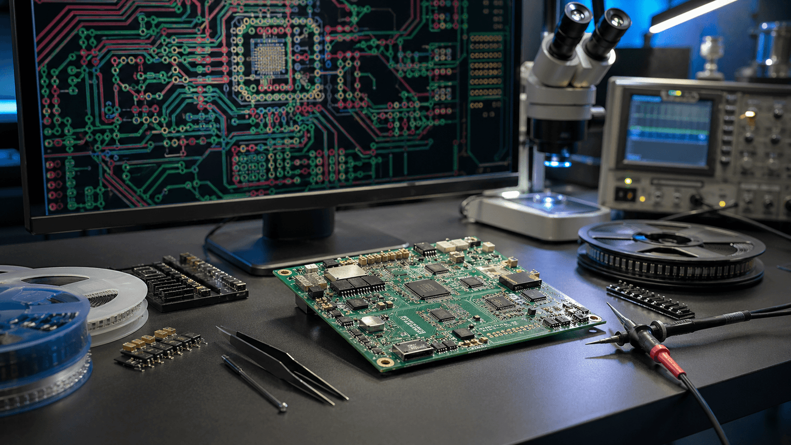
What Does a PCB Designer Actually Do?
The job title can be misleading. “Design” suggests creativity, which is accurate – but the discipline is equally analytical. A PCB designer takes an electrical schematic (a logical representation of a circuit) and physically realises it on a board that will be manufactured, assembled, and tested in the real world. That process involves far more than drawing lines between component pins.
Schematic Interpretation
Before any layout work begins, the designer must read and understand the schematic thoroughly. They need to identify power domains, understand signal hierarchies, flag ambiguities or errors in the netlist, and develop a mental model of how the circuit behaves. Experienced designers often catch schematic errors at this stage – saving significant time and cost downstream.
Component Placement
Placement is arguably the most consequential decision in PCB layout. The designer must group related components logically (e.g., keeping bypass capacitors close to their associated IC power pins), manage thermal loads, satisfy mechanical constraints (connector positions, mounting holes, keep-out zones), and set up efficient routing channels. Poor placement cannot be fixed by good routing – it will compromise the finished board.
Layer Stackup Definition
For multilayer boards, the designer defines (or works with the fabricator to define) the layer stackup – the ordering and thickness of copper and dielectric layers. Stackup decisions affect impedance control, power delivery, EMC shielding, and cost. A 4-layer board with a well-chosen stackup will outperform an 8-layer board with a poorly chosen one.
Routing
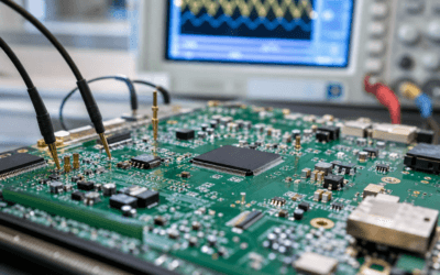
Routing is the process of drawing the copper traces that connect components according to the netlist. On simple boards this is straightforward; on high-speed digital, RF, or mixed-signal boards it demands careful attention to trace length matching, differential pair routing, controlled impedance, return path continuity, and crosstalk avoidance. The designer must also manage via placement, fanout strategies, and plane splits.
Design Rule Check (DRC) and Constraint Management
Every fabricator publishes design rules – minimum trace widths, clearances, drill sizes, annular ring requirements, and so on. A PCB designer configures these rules in their EDA tool and runs Design Rule Checks (DRC) to verify compliance before releasing the design. They also manage electrical constraints such as impedance targets and length-matching tolerances.
Design for Manufacture (DFM)
DFM is the practice of designing boards so they can be assembled and tested reliably and economically. This includes appropriate pad sizes and courtyard clearances for automated pick-and-place machines, solder mask and paste layer management, silkscreen legibility, test point accessibility, and panelisation considerations. A designer without strong DFM awareness will produce layouts that technically pass DRC but cause assembly headaches and elevated scrap rates.
Gerber and Output File Generation
The finished design is communicated to the fabricator and assembler through a package of output files: Gerber files (one per copper and mask layer), NC drill files, a bill of materials (BOM), and an assembly drawing or centroid/pick-and-place file. Errors in output generation – such as incorrect apertures, missing layers, or mis-scaled files – can result in scrapped boards or delays. Getting this step right matters.
Key Skills That Separate Great PCB Designers
EDA Tool Proficiency
The two dominant professional EDA platforms are Altium Designer and the open-source KiCad. Cadence Allegro and Mentor PADS are also used in enterprise and defence environments. Proficiency goes beyond knowing where the menus are – experienced designers use constraint managers, scripting, differential pair routing tools, and 3D clearance checking efficiently. A designer who is fluent in the tool the rest of the team uses reduces friction significantly.
Signal Integrity Awareness
As clock speeds and data rates increase, signal integrity (SI) becomes critical. A capable PCB designer understands concepts such as transmission line theory, termination strategies, via stubs and their effect on high-frequency signals, and inter-pair skew in high-speed differential interfaces (USB, PCIe, HDMI, Gigabit Ethernet). On boards running above roughly 100 MHz or with edge rates under 1 ns, SI awareness is non-negotiable.
EMC-Aware Layout
Electromagnetic compatibility (EMC) is both a regulatory requirement and a practical engineering concern. Poor PCB layout is one of the most common causes of EMC failures during pre-compliance and certification testing. A knowledgeable designer understands return current paths, the importance of solid ground planes, minimising loop areas for switching signals, and filtering placement at board entry/exit points. Designing for EMC from the outset – rather than retrofitting fixes after a failed test – saves time and money. IPC standards such as IPC-2221 provide the foundational guidelines most professional designers reference.
Thermal Management
Power dissipation must be managed through copper pours, thermal vias, component orientation, and sometimes coordination with the mechanical team on heatsinks and enclosure airflow. A PCB designer who ignores thermal considerations produces boards that overheat in the field.
DFM and DFA Knowledge
Design for manufacture (DFM) and design for assembly (DFA) knowledge comes from experience working with contract manufacturers and understanding their process constraints. This includes understanding minimum feature sizes for the chosen fabrication process, stencil design for solder paste deposition, component orientation for wave or selective soldering, and test coverage requirements. Strong DFM practice is one of the clearest markers of a seasoned designer versus a novice.
Communication and Documentation
A PCB designer must communicate clearly with electrical engineers (to clarify schematic intent), mechanical engineers (to resolve physical conflicts), fabricators (to agree on stackup and tolerances), and project managers (to report progress and flag risks). Assembly drawings, fabrication notes, and revision control discipline all fall within the designer’s remit.
PCB Layout Drafter vs Qualified PCB Designer: What Is the Difference?
The distinction matters when you are evaluating service providers.
A PCB layout drafter executes routing tasks according to instructions given by an engineer. They know how to use the tool, they can follow design rules, and they produce clean-looking boards – but they rely on others to make the engineering decisions: which stackup, which termination strategy, how to handle the power integrity of a dense BGA component, whether a particular via placement will create a stub resonance problem.
A qualified PCB designer makes those engineering decisions independently. They bring domain expertise in signal integrity, EMC, DFM, and manufacturing to the table. They can review a schematic and identify issues before layout begins. They will push back on a component choice that creates an avoidable layout problem. They take accountability for the electrical and physical performance of the finished board, not just the visual correctness of the routing.
For simple, low-speed, single-supply boards, a competent drafter may be entirely adequate. For anything involving high-speed digital signals, RF, mixed-signal design, power conversion, or a regulated product requiring EMC certification, you need a qualified designer – and ideally one backed by a broader engineering team.
Engineers Australia provides professional frameworks for recognising engineering competency; looking for designers affiliated with professional bodies or with demonstrable project histories is a practical screening approach.
When to Hire a PCB Designer vs a Full-Service Electronics Design Firm
This is one of the most common decisions hardware teams face, and the right answer depends on your situation.
Hire a Standalone PCB Designer When:
- Your schematic is complete and validated by your own engineers.
- The board is relatively straightforward – single supply, low-speed signals, no RF or high-speed interfaces.
- You have the internal capability to manage DFM review, procurement, and assembly coordination yourself.
- You need to augment capacity rather than fill a capability gap.
Engage a Full-Service Electronics Design Firm When:
- You need schematic design, PCB layout, firmware, and prototyping under one roof – with a single point of accountability.
- The product is complex: high-speed digital, RF, power electronics, IoT connectivity, or mixed-signal.
- You are targeting regulatory certification (CE, FCC, RCM) and need compliance-aware design from the start.
- You want a partner who can take the project from concept through to production – not just deliver Gerber files.
- Your team lacks the internal expertise to manage an external PCB designer effectively.
For most founders and product managers building a new hardware product, a full-service firm delivers better outcomes. The integration between schematic design, PCB layout, firmware, and DFM is tight – when the same team handles all of it, problems surface earlier and get resolved faster.
Zeus Design’s PCB Design Capability
Zeus Design is an Australian electronics design firm based in Sydney. Our circuit board design and PCB layout capability covers the full spectrum – from simple single-sided boards through to complex multilayer designs with high-speed digital interfaces, RF integration, and demanding DFM requirements.
We work in Altium Designer and handle the complete output package: Gerbers, drill files, BOM, assembly drawings, and fabrication notes. Our design process incorporates signal integrity review, EMC-aware layout practices, and DFM checks as standard – not as optional add-ons.
Because our PCB design capability sits within a broader electronics design service, we can handle schematic capture through to layout in the same team, maintaining design intent throughout. We also offer rapid PCB prototyping so that designs can be validated quickly before committing to production volumes.
We work with startups, established product companies, and engineering teams across Australia who need quality PCB design delivered on schedule.
FAQs
What qualifications does a PCB designer need?
There is no single mandated qualification for PCB designers, though most professionals hold a background in electrical engineering, electronics engineering technology, or a related discipline. Practical experience, a strong portfolio of completed designs, and familiarity with IPC standards (particularly IPC-2221 for general PCB design and IPC-2141 for controlled impedance) are typically more indicative of capability than formal credentials alone. In Australia, membership of Engineers Australia signals a commitment to professional standards.
How long does PCB design take?
Duration depends heavily on board complexity. A simple 2-layer board with a complete, clean schematic might be laid out in two to five days. A complex multilayer board with high-speed interfaces, dense component placement, and strict impedance requirements can take two to six weeks or more. DFM review, design iterations, and output file verification add time but are worth the investment before ordering prototypes.
What is the difference between PCB design and PCB manufacturing?
PCB design is the engineering process of producing the layout data – Gerber files, drill files, and documentation – that describes the board. PCB manufacturing (fabrication) is the physical process of producing bare boards from that data, typically involving lamination, etching, drilling, plating, and surface finishing. They are distinct activities, usually performed by different specialists or organisations. Assembly (soldering components onto the bare board) is a third step.
Do I need a PCB designer or an electronics engineer?
If you have a validated schematic and need it converted to a manufacturable layout, a PCB designer may be sufficient. If you need a circuit designed from scratch – component selection, schematic capture, power architecture, signal chain design – you need an electronics engineer. For most new product development, you need both: an engineer to design the circuit and a qualified PCB designer (often the same person or a closely integrated team) to realise it in layout.
What software do professional PCB designers use?
Altium Designer is the most widely used professional EDA tool in Australia and globally, valued for its integrated schematic, layout, and simulation environment. KiCad is a capable open-source alternative gaining significant adoption. Cadence Allegro and Mentor PADS are common in enterprise and defence contexts. Fusion 360 Electronics (formerly Eagle) suits simpler designs and hobbyist use. The choice of tool matters less than the designer’s depth of expertise and the tool’s suitability for your board’s complexity.
What is DFM and why does it matter in PCB design?
Design for manufacture (DFM) refers to design practices that ensure a PCB can be assembled and tested reliably and cost-effectively. DFM considerations include pad geometry for SMD components, solder mask expansion, fiducial marker placement, component spacing for pick-and-place clearances, test point accessibility, and panelisation. Poor DFM can cause assembly defects, elevated scrap rates, and costly board respins. A PCB designer with strong DFM knowledge builds these practices into the layout from the start rather than treating them as an afterthought.
How much does PCB design cost in Australia?
PCB design costs vary widely depending on board complexity, layer count, feature density, and the designer’s or firm’s experience level. Freelance designers may charge anywhere from AU$50 to AU$200+ per hour. Full-service design firms typically quote on a project basis. For a product-grade design with DFM review, signal integrity consideration, and proper output documentation, investing in quality upfront is substantially cheaper than correcting problems discovered at the prototype or certification stage.
Ready to Work with a PCB Designer?
Whether you have a schematic ready for layout or need a design partner to take your product from concept through to production-ready boards, Zeus Design’s team is available to discuss your project. We offer PCB design as a standalone service and as part of our end-to-end electronics design capability – so the engagement can be scoped to what you actually need.
")


0 Comments