
Electronics product development is the end-to-end process of turning a hardware concept into a manufacturable, market-ready product – and for Australian startups, founders, and product teams, getting that process right is the difference between a successful launch and a costly redesign. This guide walks through every stage of the hardware development journey, from initial brief and feasibility assessment through circuit design, firmware, compliance, design for manufacture (DFM), and pilot production, with practical cost and timeline benchmarks for the Australian market.
TL;DR
- Electronics product development follows a defined sequence: brief -> feasibility -> concept design -> prototype -> compliance -> DFM -> pilot production.
- Skipping or rushing early stages (especially feasibility and DFM) is the leading cause of costly late-stage redesigns.
- Australian hardware startups should budget $30,000-$150,000+ for full development depending on complexity, with timelines of 6-18 months to pilot production.
- Compliance (RCM, FCC, CE) must be planned from day one – retrofitting compliance is expensive and often forces a respin.
- Firmware and embedded software should be developed alongside hardware, not after, to avoid integration delays.
- A single integrated team covering electronics, firmware, mobile app and cloud reduces handover risk and compresses schedules.
- Zeus Design provides end-to-end electronics and software product development services from Sydney, with experience across IoT, medical, industrial and consumer electronics.
Who This Guide Is For
This guide is written for Australian hardware startups, product founders, and R&D teams who are taking an electronics product from idea to market for the first time – or who want to understand how a structured development process reduces risk and cost. Whether you have a napkin sketch or a partially developed prototype, understanding the full pipeline helps you make better decisions about timelines, budgets, and the right development partners.
If you are also looking for a deeper dive into the design engineering side, our guide to electronics design from concept to production covers circuit design, PCB layout, and compliance in greater depth.
The Hardware Product Development Stages
Most successful hardware products follow the same fundamental sequence. The stages below reflect industry best practice – aligned with frameworks used by the Australian Government’s Entrepreneurs’ Programme and leading electronics design consultancies.
Stage 1: Product Brief and Requirements
Every development engagement starts with a product brief. This document captures what the product must do, who it is for, how it will be used, what environment it will operate in, and what regulatory markets it must be certified for. A well-structured brief includes functional requirements, performance targets, target bill-of-materials (BOM) cost, production volume, and any constraints around size, power, or connectivity.
Investing a week or two in a thorough brief prevents scope creep and misaligned prototypes later. At Zeus Design, we work through this collaboratively with clients before any design work begins.
Stage 2: Feasibility Assessment
Feasibility covers technical viability, commercial viability, and regulatory risk. Key questions include: Can the product be built with available components? Does the technology exist to meet the performance targets? What compliance marks are required (RCM for Australia, FCC for the US, CE for Europe)? Are there supply chain risks for key components?
A good feasibility study also surfaces any IP considerations, identifies the highest-risk technical challenges early, and sets realistic timeline and budget expectations. For IoT and wireless products, this is where antenna strategy and spectrum licensing questions are resolved.
Stage 3: Concept Design and Architecture
With requirements locked, the engineering team produces a system architecture: the block diagram of hardware subsystems, the selection of microcontroller or processor, power management approach, communication interfaces, sensor and actuator selection, and the software stack structure. At this stage, mechanical envelope constraints are defined and handed off to any industrial design or enclosure partner.
Component selection during architecture is critical. With ongoing global component shortages, choosing widely available, multi-sourced components from the outset protects you from production delays. Lead times on some microcontrollers and RF modules have stretched to 52 weeks or more in recent years.
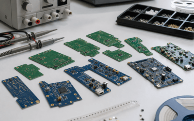
Stage 4: Schematic Design and PCB Layout
Schematic design translates the system architecture into a detailed circuit – every component, every connection, every protection circuit, and every test point. The schematic is the single source of truth for the product’s electronics and must be reviewed for correctness, reliability, and compliance requirements before PCB layout begins.
PCB layout converts the schematic into a physical board. For modern products this typically means multilayer boards with careful attention to signal integrity, EMC (electromagnetic compatibility), thermal management, and design-for-manufacture rules. EMC-aware layout is not optional – it directly affects whether the product passes compliance testing on the first attempt. Our circuit board design service covers schematic through to production-ready Gerber files, with DFM checks built into the process.
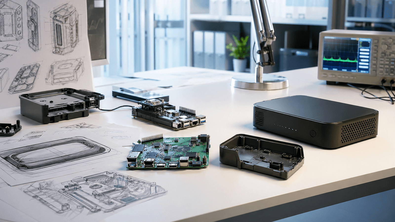
Stage 5: Rapid Prototyping and Validation
Prototyping is where the design meets reality. The first prototype – sometimes called an engineering validation test (EVT) unit – is built to validate that the hardware functions as intended. This is deliberately an imperfect build: the goal is to learn as fast as possible, not to produce a polished product.
Typical EVT activities include: powering up and measuring quiescent and peak currents; validating communication interfaces; testing sensors and actuators; confirming firmware boots and peripheral drivers work; and stress-testing thermal behaviour. Issues found at EVT are cheap to fix. Issues found at compliance testing or during manufacturing are not.
Zeus Design’s rapid electronics and PCB prototyping service covers quick-turn PCB fabrication and assembly, functional testing, and iteration support – typically delivering first prototypes within 2-4 weeks of finalised design files.
Stage 6: Firmware and Embedded Software Development
Firmware is the software that runs directly on the product’s microcontroller or processor. It controls hardware peripherals, manages power states, handles communication protocols, implements application logic, and provides over-the-air (OTA) update capability for connected products. Firmware quality is non-negotiable: a firmware bug in a shipped product can mean a costly recall or a silent failure in the field.
Best practice is to develop firmware in parallel with hardware – using hardware abstraction layers (HALs) and simulation environments where physical hardware is not yet available. This parallel development approach compresses overall project timelines significantly.
For IoT and connected products, the software stack extends beyond firmware to mobile apps and cloud backends. Zeus Design’s embedded software and full-stack development service covers firmware, desktop tools, web dashboards, mobile apps, and cloud integration as a single, cohesive engagement – eliminating the integration risk that comes from using separate vendors for each layer.
Stage 7: Compliance and Certification
In Australia, most electrical products require the Regulatory Compliance Mark (RCM), which covers both electrical safety and electromagnetic compatibility. Products with wireless interfaces also require ACMA compliance. Products destined for export markets require additional marks: FCC (USA), CE (Europe), IC (Canada), and others.
Compliance testing is performed by accredited test laboratories. Pre-compliance testing – using your own equipment or a hired EMC facility – is strongly recommended before formal submission. A single compliance test failure that requires a PCB respin can add $20,000-$50,000 and 2-4 months to a project.
Standards Australia publishes the relevant Australian Standards (notably the AS/NZS CISPR and AS/NZS 4268 series for EMC and radio). Engineers Australia also provides guidance on professional engineering practice for product certification.
Stage 8: Design for Manufacture (DFM) and Design for Test (DFT)
DFM review is a structured process of checking that the PCB and product can be reliably assembled at scale. Key checks include: component placement clearances for pick-and-place machines; solder paste aperture sizes; board panelisation; courtyard violations; and BOM rationalisation to reduce unique component counts. DFM issues that slip through to production cause yield problems, rework cost, and schedule delays.
DFT (design for test) ensures every unit can be validated during manufacturing. This typically means designing test points into the PCB and developing a custom test jig that connects to those points and runs automated functional tests on every board. A well-designed test jig pays for itself many times over in reduced escapes and warranty returns.
Stage 9: Pilot Manufacturing
Pilot manufacturing – sometimes called design validation test (DVT) or production validation test (PVT) – is a small-volume production run (typically 10-100 units) using production-representative tooling, processes, and supply chain. The goal is to prove that the product can be manufactured consistently, that the test jig catches defects, and that the firmware and software are production-ready.
For Australian startups, pilot manufacturing is often performed offshore (typically in mainland China or Taiwan) with a local engineering team managing the relationship and conducting incoming inspection. AusIndustry’s Entrepreneurs’ Programme offers matched funding for eligible commercialisation activities, which can include manufacturing setup costs.
Key Risks in Electronics Product Development
Scope Creep
Feature additions after architecture sign-off are the single biggest driver of cost and schedule overruns. Implement a formal change control process from day one. Every new requirement should be evaluated against timeline, budget, and compliance impact before being accepted.
Component Obsolescence and Shortage
Global semiconductor supply chains remain volatile. Design with multi-sourced, widely available components where possible. For any single-source components, hold safety stock or design in a pin-compatible alternative from the start.
Compliance Failures
Compliance is not a box to tick at the end – it is an engineering discipline that starts at schematic level. Build EMC review and pre-compliance testing into the project plan, not as an afterthought.
Firmware Integration Delays
Firmware developed separately from hardware consistently causes integration delays. Parallel development with continuous hardware-software integration testing eliminates the “it works on the bench but not in the product” problem.
Manufacturing Partner Alignment
Contract manufacturers need clean design packages: complete Gerber files, accurate BOM with approved vendor lists (AVLs), assembly drawings, test procedures, and packaging specifications. Incomplete handover packages are a leading cause of first-article failures.
Cost and Timeline Expectations in Australia
Cost and timeline vary significantly with product complexity, but the following benchmarks are reasonable for Australian hardware startups in 2026:
| Project Type | Typical Budget Range | Timeline to Pilot |
|---|---|---|
| Simple IoT sensor / data logger | $30,000 – $60,000 | 4 – 8 months |
| Mid-complexity connected product (wireless, app, cloud) | $60,000 – $120,000 | 8 – 14 months |
| High-complexity product (industrial, medical, multi-board) | $120,000 – $300,000+ | 12 – 24 months |
These figures cover engineering services only and exclude compliance testing fees (typically $5,000-$25,000), tooling, and manufacturing costs. Compliance testing duration can add 4-12 weeks depending on the testing lab’s queue and any failure-and-retest cycles.
Government support is available: the Entrepreneurs’ Programme from the Australian Government provides matched funding and expert facilitation for eligible businesses commercialising new products.
Zeus Design’s End-to-End Product Development Process
Zeus Design provides electronics product development services for Australian startups, scale-ups, and established businesses – from initial brief through to pilot manufacturing support. Our process is structured around five key phases:
- Discovery and Scoping – We work with you to document requirements, identify technical risks, and produce a fixed-scope Statement of Work with clear milestones and deliverables.
- System Architecture and Component Selection – Our engineers define the hardware architecture, select components with supply-chain resilience in mind, and plan the firmware and software stack in parallel.
- Design and Prototyping – Schematic, PCB layout, firmware development, and rapid prototyping proceed in integrated sprints. We deliver functional prototypes and report on test results at each EVT milestone.
- Compliance and DFM – Pre-compliance EMC review, compliance planning, DFM check, and test jig design are completed before handover to manufacturing.
- Pilot Production Support – We prepare and quality-check the manufacturing package, support the first production run, and manage incoming inspection and any required corrective actions.
How Zeus Design’s Services Connect
Hardware product development rarely ends at the PCB. Most modern products require firmware, a mobile app, a cloud backend, or all three. Zeus Design’s services are designed to work as an integrated stack:
- Electronics Design – End-to-end hardware development: circuit design, PCB layout, compliance, DFM, and production readiness.
- Rapid Prototyping – Quick-turn functional prototypes for early validation and investor demonstrations.
- Embedded Software and Full-Stack Development – Firmware, embedded Linux, cloud backends, web dashboards, and desktop device tools developed alongside the hardware.
- Mobile App Development – iOS and Android apps with IoT connectivity, cloud sync, and UI/UX optimised for hardware product workflows.
Having a single team across all these layers means no handover gaps, no finger-pointing between vendors, and a much shorter path from prototype to production-ready product.
FAQs
How long does electronics product development take in Australia?
Most electronics product development projects take 6-18 months from initial brief to pilot manufacturing, depending on complexity. A simple IoT device with one PCB and a companion app typically takes 6-10 months. A complex industrial or medical product with multiple subsystems, custom firmware, and multi-market compliance can take 18-24 months. The biggest schedule risks are compliance failures requiring a PCB respin, and component lead-time surprises.
What does electronics product development cost?
Engineering costs for hardware product development in Australia typically range from $30,000 for a simple sensor device to $300,000 or more for a complex, multi-board product with full software stack. These figures exclude compliance testing ($5,000-$25,000), tooling, and unit production costs. Government grants through the Entrepreneurs’ Programme can offset a portion of eligible commercialisation costs.
Do I need to handle compliance before manufacturing?
Yes – compliance certification (RCM in Australia, FCC in the USA, CE in Europe) must be completed before products can be legally sold in those markets. Compliance should be planned from the schematic stage, not treated as a final step. Pre-compliance testing during prototype iteration is strongly recommended to avoid costly failures at formal testing.
Should firmware be developed before or alongside hardware?
Firmware should be developed in parallel with hardware wherever possible. Waiting until hardware is complete before starting firmware adds months to the project and often reveals integration issues that require hardware rework. Using hardware abstraction layers and simulation environments allows firmware development to begin early, with progressive integration as hardware prototypes become available.
What is design for manufacture and why does it matter?
Design for manufacture (DFM) is the process of reviewing and refining electronics and PCB designs to ensure they can be assembled reliably and cost-effectively at production volumes. DFM covers component placement, soldering process compatibility, panelisation, BOM rationalisation, and test point design. Skipping DFM review is a leading cause of yield problems, assembly defects, and unexpected cost increases at the manufacturing stage.
Can Zeus Design manage the full product development process?
Yes. Zeus Design provides end-to-end electronics product development from initial brief through to pilot manufacturing support. Our team covers circuit design, PCB layout, embedded firmware, mobile apps, cloud backends, compliance planning, DFM review, and test jig development – all under a single project management structure with clear milestones and deliverables.
What types of products does Zeus Design develop?
Zeus Design has experience across IoT and connected devices, industrial monitoring and control systems, consumer electronics, medical-adjacent devices, agricultural technology, and custom embedded systems. We work with Australian startups, scale-ups, and established businesses that need specialist electronics and software engineering capability without the overhead of building an in-house team.
Ready to Start Your Product Development?
Whether you have a fully specified product brief or just an idea you want to pressure-test, Zeus Design can help you define, design, and deliver your electronics product. We work with Australian hardware startups and product teams who need an experienced, integrated engineering team – not a chain of disconnected contractors.


0 Comments