
This guide explains what quality electronic design services look like in practice – covering schematic design, PCB layout, firmware development, design for manufacture and compliance – so Australian product teams and hardware startups can evaluate a development partner with confidence and avoid the most common engagement mistakes.
TL;DR
- A credible electronics design partner covers the full scope: schematic capture, PCB layout, embedded firmware, DFM, compliance planning and production handover – not just one layer.
- Schematic quality is the foundation. Errors here cascade into PCB respins, firmware bugs and failed compliance tests.
- DFM and pre-compliance work should start during layout, not after the first batch of prototypes comes back wrong.
- In Australia, RCM (Regulatory Compliance Mark) certification is mandatory for most electronic products sold commercially. Your partner should design with this in mind from day one.
- Deliverables matter as much as the design itself – insist on Gerber files, full BOM with manufacturer part numbers, firmware source, test documentation and production-ready files.
- The best partnerships integrate electronics design, embedded software and connectivity work under one roof to avoid interface failures between teams.

Why the Scope of “Electronic Design Services” Matters
Most product teams engaging an electronics design firm for the first time underestimate what a complete engagement covers. They expect PCB layout. What they actually need is a coordinated process that starts with architecture decisions and ends with a production-ready package their contract manufacturer can use without coming back to ask questions.
When that scope is fragmented – one firm does schematics, another does layout, a freelancer handles firmware – the handoff gaps are where projects get into trouble. Signal integrity issues that a layout engineer would catch are missed because the schematic engineer is not watching. Firmware assumptions about hardware behaviour create bugs that take weeks to isolate. Compliance problems surface in testing because nobody was thinking about EMC during placement.
For Australian founders and engineering managers evaluating a development partner, the key question is not “can they design a PCB?” It is “do they understand the whole chain from requirement to production, and can they manage the risks at each stage?”
This guide covers each layer of that chain – what it includes, what a quality partner delivers, and where the commercial and technical risks sit.
What Electronic Design Services Include
Schematic Design and Circuit Architecture
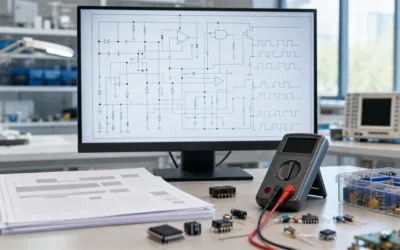
Schematic design is where a product’s electrical behaviour is defined. A quality partner translates your functional requirements into a circuit architecture: power supply topology, microcontroller selection, analogue signal conditioning, communication interfaces, protection circuits and component selection.
Component selection at this stage has long downstream consequences. Parts chosen without considering supply chain availability, lifecycle status, production cost and footprint availability create problems at exactly the wrong time – usually during scale-up. A partner with production experience brings this discipline to schematic work from the start.
Deliverables at this stage should include a schematic PDF and native design files (typically Altium, KiCad or Cadence), a preliminary bill of materials with manufacturer part numbers, and a design review sign-off before layout begins. Requiring a second engineer to peer-review the schematic – not just the designer – is a mark of a serious firm. Altium’s PCB design documentation outlines the constraint-driven workflow that professional-grade tools support.
PCB Layout and Signal Integrity
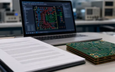
PCB layout translates the schematic into a physical board. The decisions made during layout – layer stack-up, component placement, trace routing, power plane design, thermal management and via strategy – directly determine whether the finished board works as intended, passes compliance testing and can be manufactured reliably at volume.
Common failure points include inadequate impedance control on high-speed signal lines, poor ground plane continuity causing EMC issues, thermal bottlenecks that shorten component life, and placement decisions that create assembly problems. None of these are visible in a rendered board image – they show up in testing, in the field or in a compliance lab.
A quality electronics partner applies design rules that match the manufacturing capability of their preferred fabricators, includes a design rule check (DRC) pass before releasing files, and produces a complete manufacturing package: Gerber files, drill files in Excellon format, a pick-and-place centroid file, assembly drawings and a 3D STEP model for mechanical integration.
For multilayer boards – four layers and above – the layer stack-up should be documented explicitly, particularly where differential pairs, impedance-controlled traces or high-current planes are involved.
Embedded Software and Firmware Development
For most products, the electronics and the firmware are inseparable. A board that works electrically can still fail because the firmware does not correctly initialise peripherals, manage power states or handle edge cases in communication protocols.
When electronics design and embedded software development are handled by the same team, hardware-software co-design is possible: the firmware engineer can influence pin assignments, interrupt architecture and peripheral configuration before the PCB is finalised, rather than adapting to whatever the hardware turned out to be.
Firmware deliverables should include source code in a version-controlled repository, documentation of the build environment and toolchain, binary files for production flashing, and a test harness or diagnostic mode that allows production testing without custom equipment at early stages.
For connected products, security matters. Secure boot, firmware update mechanisms, encrypted communication and key management should not be retrofitted – they need to be designed in. OWASP’s Embedded Application Security guidance is a useful reference for what a production-grade firmware security posture looks like.
IoT Connectivity
Products with wireless connectivity – Wi-Fi, Bluetooth, Cellular, LoRaWAN or other LPWAN protocols – introduce additional design and compliance complexity. Antenna design and placement, RF shielding, co-existence between multiple radios, and power budget management for battery-operated devices all require deliberate engineering attention.
Using a certified module (such as an ESP32 module with FCC/CE certification) versus designing a custom RF front end has significant implications for both compliance cost and board real estate. A partner with connectivity experience can advise on the right trade-off for your production volume and certification timeline.
Zeus Design’s electronics design service covers IoT connectivity design as part of the hardware scope, including selection of appropriate wireless technology and integration with cloud back-end systems where required.
Design for Manufacture (DFM)
Design for manufacture means designing the product so it can be assembled reliably, tested efficiently and scaled to production volume without continuous engineering support. DFM is not a final review step – it is a design discipline that should be applied throughout layout.
Key DFM considerations include component courtyard clearances for pick-and-place machinery, appropriate solder mask and paste mask definitions, testpoint placement for in-circuit testing, panelisation strategy, conformal coating accessibility and component orientation consistency to reduce assembly errors.
Skipping DFM review on early prototypes creates a false sense of readiness. A board that works when hand-assembled by the engineer who designed it can fail frequently in production assembly if DFM has not been applied. The rework cost – respinning the board, re-qualifying firmware, re-testing – is typically far higher than addressing DFM issues in the layout phase.
Compliance and Pre-Certification Planning
In Australia, the law requires electronic products sold commercially to carry the Regulatory Compliance Mark (RCM), which covers both electrical safety and electromagnetic compatibility (EMC) requirements managed jointly by the Australian Communications and Media Authority (ACMA) and Energy Safe Australia. The Electrical Equipment Safety System (EESS) provides the regulatory framework for RCM registration and supplier obligations.
Compliance failure is expensive. ACMA enforcement powers include financial penalties up to AUD 165,000 per offence, product recalls and supply prohibitions. A redesign triggered by EMC test failure – after prototypes are built and firmware is written – can add months and significant cost to a project on top of any regulatory exposure. Pre-compliance design practices – careful ground plane design, filtering on switching supplies, proper trace routing for high-frequency signals, attention to cable entry points – significantly reduce the risk of first-attempt test failure.
A quality electronics design partner plans for the target compliance marks from the start of the project. This means selecting components and modules with appropriate certifications, designing for the relevant test standards, and flagging decisions that could create compliance risk before they are locked into the layout.
For products that also require CE marking for European markets or FCC authorisation for the US, the same planning discipline applies – ideally with the compliance strategy defined before schematic work begins.
When a Project Needs a Full-Service Electronics Design Partner
Not every project requires an end-to-end electronics design engagement. A company with in-house PCB designers who need firmware support has different needs from a startup with a concept but no engineering team.
Situations where a full-service partner adds the most value include:
- New product development from concept – where architecture decisions, component selection and development risk management require broad experience, not just execution capability.
- Products with wireless connectivity – where electronics design, firmware and cloud connectivity need to be co-designed to avoid interface failures.
- Products heading to regulatory compliance testing – where pre-compliance planning during design is worth significantly more than post-failure redesign.
- Startups without in-house engineering – where the partner effectively acts as the product engineering team, covering technical decisions the client cannot yet make internally.
- Companies scaling from prototype to production – where DFM, test jig development, production documentation and supply chain support are needed alongside the design work.
Zeus Design’s rapid prototyping service provides early-stage validation builds for teams that need to prove out a concept before committing to a full development engagement.
Technical and Commercial Risks to Manage
Component Availability and Supply Chain Risk
The disruptions of recent years made it clear that component availability is a design decision, not a procurement problem. A partner that specifies components with limited second-source options, long lead times or approaching end-of-life creates supply risk that becomes your problem at the worst possible moment – typically when you are trying to ramp production.
Responsible electronics design services include BOM review for supply chain risk: identifying single-source components, checking distributor stock levels and lead times, confirming lifecycle status, and suggesting alternatives where risk is high. This is especially important for microcontrollers, power management ICs and wireless modules, which are historically the most constrained categories.
Scope Creep and Requirements Drift
Electronics design projects frequently expand scope during development. A new feature request late in the layout phase can require moving significant board real estate, changing the layer count or redoing power budget calculations. Without clear requirements documentation and a defined change management process, cost and timeline overruns are predictable.
Before engagement, confirm the partner’s process for managing requirement changes: how changes are documented, how they are priced, and who approves them. A partner that can articulate this clearly is operating with engineering discipline; one that cannot is likely to absorb or ignore scope changes until they create a problem.
Intellectual Property Ownership
Confirm upfront who owns the design files, schematic source, PCB native files and firmware source code. In Australia, IP ownership in a commissioned work defaults to the creator unless a written agreement transfers it to the client. A contract that provides full IP transfer on completion – including native design files, not just Gerber outputs – protects your ability to work with other suppliers in future, make design changes internally and move to production without dependency on the original firm.
Documentation Gaps
Many electronics design engagements produce a working prototype but incomplete documentation. If the engineer who designed it leaves, or if you need to hand the project to a contract manufacturer or a different development firm, incomplete documentation creates significant cost and delay. Insist on a defined deliverables list before engagement starts, and ensure it includes all the files a third party would need to manufacture, test and support the product.
Zeus Design’s Process and Deliverables
Zeus Design is an Australian electronics and software design firm covering electronics design, PCB and circuit board design, embedded software, IoT connectivity, rapid prototyping, design for manufacture, compliance planning and test jig development. Engagements are structured end-to-end, not as component services – hardware, firmware and connectivity are developed as an integrated system rather than handed between separate teams.
The engagement process typically follows this sequence:
- Requirements and architecture – define functional requirements, electrical architecture, technology selection and compliance targets before schematic work begins.
- Schematic design and review – circuit design with peer review and client sign-off before layout.
- PCB layout – DFM-aware layout with signal integrity and compliance design practices applied throughout.
- Firmware development – hardware-software co-design where firmware is developed alongside the PCB, not after it.
- Prototyping and testing – functional validation, pre-compliance checks and iteration before production commitment.
- Production handover – complete manufacturing package, test documentation, BOM and DFM sign-off for contract manufacturer handover.
Deliverables include schematic PDFs and native design files, full manufacturing Gerber/drill/BOM/assembly packages, firmware source in version control, test procedures and jig documentation, and production-ready design files suitable for direct handover to a contract manufacturer.
For connected and IoT products, the scope extends to cloud and software development where back-end systems, APIs and device management infrastructure need to be built alongside the hardware.
How Electronic Design Connects to Related Services
Electronics design rarely exists in isolation. The hardware needs firmware to run, the firmware often needs a mobile app or cloud platform to be useful, and the manufacturing process needs test infrastructure to ensure quality at scale.
The services that most commonly extend a core electronics design engagement include:
- Embedded software and firmware – developed in parallel with hardware for reliable integration and faster validation cycles.
- IoT connectivity and cloud back-end – for connected products that need device management, data storage, APIs or real-time monitoring.
- Mobile app development – for products controlled or monitored via iOS or Android, including Bluetooth and Wi-Fi pairing flows.
- Test jig development – custom test fixtures for repeatable production testing, particularly important for volume builds where manual test procedures are not cost-effective.
- Rapid prototyping – early-stage proof-of-concept builds before full development commitment, used to validate architecture and de-risk the main engagement.
Keeping these services integrated – rather than managing separate relationships for each – reduces the communication overhead and interface risk that fragment multi-vendor projects.
FAQs
What does an electronic design services engagement typically cost in Australia?
Costs vary significantly with project scope and complexity. Based on Zeus Design project experience, a simple single-board product with basic firmware typically runs from AUD 15,000 to AUD 40,000 for a complete design engagement. A complex multi-board product with wireless connectivity, cloud integration and regulatory compliance support can reach AUD 80,000 to AUD 200,000 or more. The more useful framing is to ask what it costs to get a production-ready package, not just a working prototype – the two can be very different numbers.
How long does an electronic design services project take from concept to production-ready files?
Based on Zeus Design project experience, a straightforward product with modest complexity – single PCB, no wireless, basic firmware – typically reaches a production-ready state in three to five months. A connected IoT product with cloud integration, mobile app and compliance certification can take nine to eighteen months or longer, depending on compliance testing timelines and iteration cycles. Pre-compliance planning during design is the single biggest factor in avoiding timeline blowouts from test failures.
Do I need RCM certification for my electronic product in Australia?
Most electronic products sold commercially in Australia require the Regulatory Compliance Mark (RCM), which covers both electrical safety and EMC requirements. The ACMA requirements for RCM use set out the specific obligations, including supplier registration on the national database and record-keeping for up to ten years. Your design partner should be designing with RCM requirements in mind from the schematic stage, not flagging compliance as an afterthought after prototypes are built.
What files should I receive at the end of an electronic design engagement?
A complete deliverables package should include: schematic PDF and native design files (Altium, KiCad or similar), Gerber and drill files for PCB fabrication, pick-and-place centroid file, full BOM with manufacturer part numbers and distributor references, assembly drawings, 3D STEP model, firmware source code in version control with build instructions, test procedures and production test documentation. If you do not receive native design files (not just Gerbers), you have limited ability to make changes without returning to the original firm.
Should electronics design and firmware development be done by the same firm?
In most cases, yes. Hardware-software co-design – where firmware engineers are involved in hardware decisions before the PCB is finalised – produces more reliable products and faster validation cycles than sequential handoffs between separate teams. The firmware engineer can influence pin assignments, interrupt architecture and peripheral selection; the hardware engineer can flag constraints that affect firmware complexity. Separate firms working in sequence miss these optimisation opportunities and create integration risk at handoff.
How do I evaluate whether an electronics design partner has the right experience?
Ask to see examples of completed projects in similar product categories – not renders, but evidence of boards that went through prototyping, testing and production handover. Ask specifically about their DFM process, their compliance design practices, and how they manage component supply chain risk in the BOM. A partner that can speak concretely to these topics – with specific examples – is operating with production-grade discipline. One that deflects with general capability claims is worth further scrutiny. Zeus Design’s electronics design service page outlines the scope of what a full engagement covers.
Conclusion
Quality electronic design services deliver more than a board that powers on. They deliver a production-ready system – from a validated schematic through compliant PCB layout, integrated firmware, DFM documentation and a complete manufacturing package – that allows a product to move from prototype to production without constant re-engagement with the development team.
For Australian product teams, the additional dimension is compliance. Designing for RCM from the start, rather than discovering EMC or safety issues in the test lab, is the difference between a smooth certification process and an expensive redesign cycle.
The right partner integrates electronics design, embedded software and connectivity work as a single discipline – not as separate services requiring coordination overhead. That integration is where the risk reduction and timeline improvements actually come from.




0 Comments