Custom electronics development is the process of designing and building electronic hardware tailored to a specific product requirement – and for startups and product companies, understanding how it works from brief to build determines whether a project stays on schedule and on budget. This guide is written for founders, product owners and engineering managers who are either entering the custom electronics development process for the first time or reviewing it before engaging a design partner. It covers how to define your requirements, what happens at each development stage, and where Zeus Design’s electronics design and rapid prototyping services fit into the process.
TL;DR
- Custom electronics development spans requirements definition, circuit and PCB design, firmware, prototyping and production preparation – each stage gates the next.
- A well-written brief reduces scope creep and rework; most project overruns originate from vague or changing requirements, not engineering errors.
- Prototyping is not a single step – expect proof-of-concept, functional prototype and pre-production iterations, each with a different purpose.
- Design for manufacture (DFM) decisions made during PCB layout directly affect production yield, unit cost and test reliability.
- Integrated design partners who handle electronics, firmware and compliance together compress timelines and reduce handover risk compared to assembling a chain of specialists.
- Zeus Design provides end-to-end custom electronics development from Sydney, including electronics design, rapid prototyping, embedded software and DFM support.
Who This Guide Is For
If you have a product idea that requires custom hardware – a connected sensor, an industrial controller, a medical device, a consumer IoT product, or any electronics that needs to be built from scratch rather than bought off the shelf – this guide explains what the development process actually looks like. It is aimed at non-engineers and technically aware founders who need to brief, manage and evaluate a custom electronics development engagement, not write the code or design the schematic themselves.
The Australian hardware startup and product development landscape has grown significantly, with government manufacturing and innovation initiatives supporting local product development. However, many founders still approach the brief with insufficient detail, which leads to misaligned scope, budget overruns and delayed first prototypes. Getting the brief right is where most successful projects diverge from struggling ones.
What Custom Electronics Development Includes
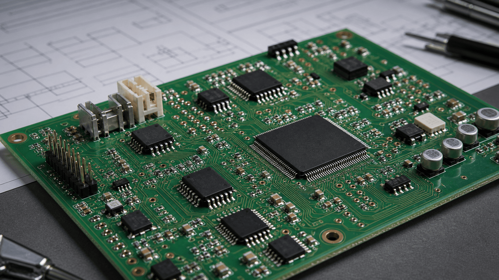
Custom electronics development is not a single deliverable – it is a staged process where each phase produces outputs that feed the next. A complete engagement typically covers the following disciplines:
- Requirements and feasibility: Translating a product concept into a technical specification, including electrical requirements, power budget, connectivity, environmental conditions, compliance targets and production volume expectations.
- Circuit design and schematic capture: Designing the electrical architecture – selecting components, defining signal paths, power supply topology, protection circuits and interfaces. This is where electrical performance, cost and reliability are largely determined.
- PCB layout and design for manufacture: Converting schematics into a manufacturable board. Layer stack, component placement, signal routing, thermal management and DFM rules all affect yield and cost at volume.
- Embedded firmware development: Writing the software that runs on the hardware – initialisation, peripheral drivers, communication protocols, power management, over-the-air update mechanisms and application logic.
- Prototyping and iteration: Building and testing physical hardware at proof-of-concept, functional prototype and pre-production stages to validate design decisions before committing to tooling or production runs.
- Compliance and certification planning: Designing to meet regulatory requirements such as CE, FCC, RCM and EMC standards from the start, rather than retrofitting compliance after the fact.
- Production handover: Finalising the bill of materials, Gerber files, firmware binaries, test specifications and assembly documentation for a contract manufacturer.
Zeus Design’s electronics design service covers this end-to-end process, integrating hardware and firmware development rather than treating them as separate contracts.
How to Write a Requirements Brief That Works
The brief is the single highest-leverage input in a custom electronics development project. A vague brief does not save time – it transfers the cost of unclear thinking into expensive engineering iterations later. A functional brief should include:
Product function and use case
What does the device do? Who uses it, how, and in what environment? Include operating conditions – temperature range, ingress protection, vibration, humidity – because these directly affect component selection and PCB design rules. A consumer product used indoors has different tolerances to an industrial device in a mining or marine environment.
Electrical and interface requirements
What inputs and outputs does the device need? What sensors, actuators, displays or communication interfaces are required? What are the power supply requirements – battery-powered, mains, solar, or PoE? What is the acceptable power consumption at idle and at peak? These questions are not optional detail – they define the circuit architecture from day one.
Connectivity and data requirements
Does the device need to communicate wirelessly? Via Wi-Fi, Bluetooth, cellular (LTE-M, NB-IoT), LoRaWAN or Zigbee? Does it need to push data to a cloud backend, respond to remote commands, or operate entirely offline? Connectivity decisions affect antenna design, RF compliance, power budget and firmware complexity. According to Seacomp’s electronics design guidance, connectivity architecture is one of the most commonly underspecified areas in early briefs.
Production volume and cost targets
How many units do you expect to produce in the first run, and over 12 months? Component selection, PCB layer count and assembly process choices are all influenced by volume. A 100-unit pilot run tolerates different trade-offs than a 10,000-unit production run. If you have a target unit cost, state it – it is a design constraint, not just a commercial preference.
Compliance requirements
What markets will the device sell into? Australian RCM, European CE or US FCC certification all require different testing and design controls. Starting compliance planning at the brief stage avoids costly redesigns after first prototype. Pre-compliance EMC checks during prototyping are significantly cheaper than discovering a failure during formal testing.
The Custom Electronics Development Stages
Stage 1 – Feasibility and concept definition
Before any circuit is drawn, a feasibility assessment validates whether the product concept is technically and commercially achievable within the stated constraints. This includes reviewing the requirements brief, identifying risks, sizing the development scope and providing a realistic timeline and cost estimate. The output is a development roadmap – not a fixed quote, but a structured view of phases, gates and decision points. Skipping this stage and going directly to design typically results in scope surprises within the first four weeks.
Stage 2 – Circuit design and architecture
With requirements confirmed, electrical engineers design the circuit architecture. This covers power supply design, microcontroller or SoC selection, peripheral interfaces, signal conditioning, protection circuitry and communication subsystems. A well-designed circuit is not just functional – it is optimised for the operating environment, manufacturable at the target volume, and designed with test access in mind. Component selection at this stage also determines long-term supply chain risk; engineering teams experienced in production will flag components with short lifecycle or limited availability.
Zeus Design’s circuit design capability covers analog and digital design, optimised for performance, reliability and manufacturability at volume.
Stage 3 – PCB layout and DFM
PCB layout converts the schematic into a physical board. Decisions made here – layer count, component placement, trace routing, impedance control, copper pours, via strategy, keepout zones – directly affect signal integrity, EMC performance, thermal behaviour, assembly yield and unit cost. Altium’s PCB design documentation outlines many of the DFM and signal integrity considerations that separate production-ready layouts from prototype-only designs.
DFM review at the layout stage catches issues that would otherwise show up as assembly defects, rework costs or yield losses during production. For multi-layer boards or designs with tight impedance requirements, signal integrity simulation during layout avoids costly respins. Zeus Design’s circuit board design service applies DFM rules and pre-compliance checks during layout, not as a post-design audit.
Stage 4 – Embedded firmware development
Firmware developed in parallel with hardware – rather than after first prototype – reduces integration risk and accelerates the testing cycle. Good firmware architecture at this stage includes hardware abstraction layers that make the software portable across hardware revisions, robust bootloaders for field updates, and clear separation between hardware drivers and application logic. For connected products, firmware also covers protocol stacks, security architecture and over-the-air update mechanisms.
Zeus Design’s embedded software development runs alongside electronics design so hardware and firmware are integrated from the first prototype build, not bolted together after fabrication.
Stage 5 – Prototyping and iteration
Prototyping in a professional custom electronics development process is structured, not exploratory. There are typically three meaningful prototype stages:
- Proof of concept (PoC): Validates the core function using development boards or early custom hardware. The goal is to answer the riskiest technical questions quickly – does the sensor interface work? Is the power budget achievable? Can the wireless link meet the latency requirement? – before committing to a full custom design.
- Functional prototype (Alpha): First custom PCB build. Tests the complete electrical design under real operating conditions. Firmware is functional but not final. This prototype is used to identify design issues before the next iteration.
- Pre-production prototype (Beta): Incorporates all changes from functional prototype testing. Close to final hardware. Used for regulatory pre-compliance testing, mechanical fit checks, software finalisation and production process validation.
According to Predictable Designs’ hardware development guide, the most common reason for prototype overruns is compressing these stages – treating a functional prototype as production-ready when it has not been through pre-compliance testing or DFM review.
Zeus Design’s rapid prototyping service builds functional PCB prototypes for early validation, with DFM principles applied from the first custom board to reduce iteration count before production.
Stage 6 – Compliance and pre-certification
Compliance is not a stage that happens after design is finished – it is an ongoing design constraint. The earlier compliance targets are defined, the cheaper they are to achieve. Pre-compliance EMC testing during the beta prototype stage identifies radiated and conducted emission issues before formal certification testing. This is particularly important for products with switching power supplies, wireless modules or high-speed digital interfaces, all of which are common EMC failure areas.
Australian RCM certification requirements, administered by the ACMA and aligned with relevant AS/NZS standards, apply to most electronic products supplied to the Australian and New Zealand markets. Planning for this during circuit design – not retrofitting shielding and filtering after a test failure – is the commercially correct approach.
Stage 7 – Production handover
The final stage is preparing the complete design package for a contract manufacturer. This includes finalised Gerber and drill files, assembly drawings, BOM with approved component alternatives, test specifications, firmware binaries and programming instructions, and any custom test jig documentation. A production handover that is incomplete or ambiguous typically results in delays, additional NRE charges from the manufacturer, or quality escapes in the first production run.
Test jigs developed alongside the hardware – rather than after the production build starts – ensure repeatable functional testing at the production line. Zeus Design’s test jig development capability covers fixture design and test automation integrated with the electronics design process.
Technical and Commercial Risks to Manage
Requirements drift
The most common cause of budget overrun in custom electronics development is changing requirements after design has started. Each change to the circuit architecture, connectivity design or form factor during layout or prototype stages triggers rework that compounds. Defining a change control process at the start of the engagement – and respecting it – is a commercial discipline as much as an engineering one.
Component availability
Component lead times for semiconductors, passive components and wireless modules remain unpredictable in 2026. Designs that rely on single-source components without approved alternatives carry supply chain risk that may not surface until production is planned. Experienced design teams maintain alternative component lists and check lifecycle status during component selection, not as an afterthought.
Piecemeal outsourcing
Splitting electronics design, firmware and PCB layout across separate contractors introduces interface risk – the point where one contractor’s output becomes another’s input is where integration problems are most likely to occur. A design house that integrates all disciplines reduces this risk. The handover between hardware schematic and PCB layout, and between hardware and firmware, are the two most consequential integration points in a custom electronics development project.
Underestimating prototype iteration count
Most custom electronics products require two to four prototype iterations before reaching a production-ready state. Budgeting for one prototype and hoping for a clean first pass is the most reliable way to run out of development budget before production. A professional feasibility assessment will provide a realistic iteration estimate based on product complexity and compliance requirements.
How Zeus Design Approaches Custom Electronics Development
Zeus Design handles custom electronics development as an integrated process, not a series of separate services. Electronics design, PCB layout, embedded firmware, rapid prototyping, DFM and test jig development are managed as a single engagement. This means the engineer designing the circuit also reviews the PCB layout for signal integrity and DFM compliance, and the firmware team has visibility of hardware decisions that affect driver and protocol implementation from the start.
For Australian product teams, working with a local Sydney-based design partner also reduces the coordination overhead that comes with offshore development – time zone alignment, IP protection under Australian law, and direct access to the engineering team during critical prototype phases.
Zeus Design’s relevant services for custom electronics development:
- Electronics Design – end-to-end circuit design, PCB layout, DFM and compliance support
- Rapid Electronics and PCB Prototyping – quick-turn functional prototypes for early validation
- Embedded Software Development – firmware developed alongside hardware for integrated testing
FAQs
What is custom electronics development?
Custom electronics development is the process of designing and building electronic hardware to a specific product specification, rather than adapting off-the-shelf modules. It covers circuit design, PCB layout, embedded firmware, prototyping and production preparation – typically carried out by a specialist electronics design firm or design house. The output is a manufacturable product design tailored to the buyer’s functional, compliance and cost requirements.
How long does custom electronics development take?
Timeline depends heavily on product complexity and prototype iteration count. A straightforward connected sensor with a well-defined brief might reach a functional prototype in 8-12 weeks. A complex industrial controller with multiple interfaces, custom firmware and regulatory certification may take 6-12 months from brief to production-ready handover. Feasibility assessment at the start of the project provides the most reliable timeline estimate. See Zeus Design’s rapid prototyping service for prototype timeline guidance.
How much does custom electronics development cost in Australia?
Costs vary significantly with scope. A proof-of-concept prototype engagement might start in the low tens of thousands of dollars for a simple design. A complete product development from concept to production-ready design – including multiple prototype iterations, firmware, DFM and compliance support – typically ranges from $50,000 to $200,000+ depending on complexity, regulatory requirements and production volume targets. Cost in AUD should be scoped against a detailed requirements brief for an accurate estimate.
What do I need to prepare before briefing a custom electronics development partner?
At minimum: a clear statement of what the device does, who uses it, the operating environment, power requirements, connectivity needs, any regulatory or compliance requirements, target production volume and unit cost, and your timeline. The more complete the brief, the more accurate the scope and cost estimate. A design partner should help refine requirements during feasibility, but they cannot substitute for the product team’s knowledge of the use case and commercial constraints.
What is DFM and why does it matter in custom electronics development?
Design for Manufacture (DFM) is a set of PCB design practices that make a board easier and more reliable to assemble and test at production scale. DFM decisions during layout – such as component placement, pad geometry, via-in-pad usage and testpoint access – directly affect assembly yield, production cost and test coverage. Applying DFM from the prototype stage rather than as a post-design review reduces expensive respins and avoids production defect rates that only appear at volume. More detail is available in Altium’s PCB design documentation.
Can Zeus Design handle both hardware and firmware for a custom electronics project?
Yes. Zeus Design integrates electronics design, PCB layout and embedded firmware development within a single engagement. Hardware and firmware are developed in parallel, which means firmware is running on real hardware – not simulated – from the first prototype build. This reduces integration risk and accelerates the validation cycle compared to engaging separate hardware and software contractors. See Zeus Design’s embedded software development service for detail on firmware capabilities.
How does prototyping reduce risk in custom electronics development?
Each prototype stage answers specific technical questions before the project commits to the next level of investment. A proof-of-concept validates that the core function is achievable. A functional prototype confirms the full circuit design under real conditions. A pre-production prototype validates compliance, mechanical fit and production process before tooling and volume manufacturing spend is committed. Compressing or skipping these stages transfers technical risk forward into the most expensive part of the project – production.
Conclusion
Custom electronics development follows a structured process from requirements brief to production-ready build – and the quality of the brief determines the quality of the outcome more than any other single factor. Getting requirements defined clearly, choosing a design partner who integrates hardware and firmware, and respecting the prototype iteration process are the three decisions that most reliably result in a product that ships on time, within budget and ready for manufacture.
For product teams and startups in Australia, Zeus Design provides integrated custom electronics development services from Sydney – covering electronics design, rapid prototyping, embedded software and DFM support through a single engagement. If you are planning a custom electronics project, start with a project discussion to get a realistic feasibility assessment and development roadmap before committing to a full scope.




0 Comments