
IoT device design is the hardware-layer discipline that determines whether a connected product works reliably in the field, meets Australian regulatory requirements, and ships within budget. While IoT development as a whole spans firmware, cloud and mobile, the device design phase – covering hardware architecture, wireless module selection, power supply design and sensor integration – sets the constraints that every other layer must live within. Get it right and the rest of the project is tractable. Get it wrong and no amount of clever firmware or cloud engineering can compensate for a hardware design that draws too much current, drops its wireless link under load, or fails pre-compliance testing. This guide is written for product teams and hardware startups navigating IoT device design decisions in 2026.
TL;DR
- IoT device design covers hardware architecture, microcontroller or SoC selection, wireless module integration, power supply design, sensor integration, PCB layout and compliance planning.
- Wireless protocol selection – Wi-Fi, BLE, LoRaWAN, LTE-M or NB-IoT – is the highest-leverage early decision; it drives power budget, antenna design, certification scope and cloud architecture.
- Power architecture must be modelled before schematic design begins: battery life targets flow directly into sleep current budgets, regulator selection and radio duty-cycle requirements.
- Australian radio devices must meet ACMA requirements and carry RCM marking; pre-certified wireless modules simplify certification but require careful antenna integration to remain valid.
- Sensor selection and signal conditioning are frequently underestimated; noise, offset and drift in the analogue front-end corrupt data before it ever reaches the cloud.
- The PCB layout phase – particularly antenna keepout compliance, ground plane management and decoupling – determines whether an RF-performing device passes pre-compliance testing or requires a costly board respin.
- Working with a design team that spans hardware, firmware and wireless from the outset eliminates the interface gaps that cause most IoT device failures.
Why IoT Device Design Is Harder Than It Looks
A connected sensor node seems straightforward on paper: a microcontroller, a radio, a sensor, a power source and some firmware. In practice, the interactions between these elements create a design space with far more failure modes than any component in isolation. The radio’s transmit burst draws current that collapses the supply rail if the power design has insufficient bulk capacitance. The sensor’s I2C address conflicts with the wireless module. The antenna keepout area on the PCB is violated by a mounting hole, degrading range by 6 dB. The deep-sleep current is acceptable at 20 degrees Celsius but doubles at 85 degrees due to regulator quiescent current variation.
These are not exotic edge cases – they are routine issues in IoT device design that an experienced electronics design team anticipates and manages. For product teams without that background, discovering them during prototype bring-up or, worse, pre-compliance testing, is expensive. Zeus Design’s electronics design service covers the full IoT device hardware lifecycle: architecture through PCB layout, RF integration, power design and compliance planning.
Hardware Architecture Decisions
Microcontroller vs SoC vs Module
The first architecture decision is where computation and radio capability will live. The main options are:
- Discrete microcontroller plus external wireless module – gives the most flexibility in choosing the best-fit processor and radio independently; the module handles certification of the radio subsystem. This is the most common approach for industrial IoT devices with moderate BOM cost sensitivity.
- Integrated SoC – devices like the Nordic nRF52 series (BLE), Espressif ESP32 (Wi-Fi/BLE) and Silicon Labs EFR32 (multi-protocol) integrate processor and radio in a single die. Simpler BOM, smaller footprint, but the entire RF design must be certified as part of the product.
- System-in-package (SiP) or pre-certified module – a certified module (e.g. u-blox, Murata, Nordic Thingy) contains the SoC, memory and RF front-end in a shielded package with regulatory pre-certification. Highest BOM cost per unit but lowest certification risk and fastest time to market. The right choice when volume is too low to justify custom RF design certification.
The right architecture depends on volume, cost targets, performance requirements, timeline and the team’s RF design capability. Zeus Design’s IoT hardware design practice helps product teams evaluate these trade-offs at the project start before any schematic work begins.
Memory and Storage
IoT devices often require more memory than the microcontroller’s internal flash and RAM can provide. External QSPI flash for firmware image storage and OTA update buffers, FRAM or EEPROM for persistent configuration and event logs, and external RAM for data-intensive applications all add complexity to the memory subsystem. Memory selection affects power consumption, PCB routing density and firmware architecture simultaneously.
Wireless Protocol Selection
No decision in IoT device design has more downstream consequences than wireless protocol selection. It determines the radio subsystem design, antenna type and placement, firmware stack complexity, certification scope, power budget and the cloud infrastructure the device connects to. Choosing the wrong protocol for the deployment environment is not fixable in firmware.
Wi-Fi (802.11 b/g/n/ax)
Wi-Fi provides high throughput and connects to existing infrastructure without requiring a separate network gateway. It is the right choice for mains-powered devices that need to push significant data volumes – security cameras, industrial gateways, smart appliances. Its high transmit current (typically 200-400 mA peak for 802.11n) makes it unsuitable for battery-powered field sensors without aggressive power management. Wi-Fi 6 (802.11ax) introduces target wake time (TWT) which substantially reduces power consumption for periodic-reporting IoT applications.
Bluetooth Low Energy (BLE)
BLE is optimised for short-range, low-power applications and direct connectivity to smartphones. It is the dominant protocol for wearables, medical devices, asset tags and any IoT product that pairs directly with a mobile app. BLE 5.x extended range (Coded PHY) supports distances up to several hundred metres at reduced data rate, expanding its applicability beyond the traditional 10-metre range. BLE is commonly used alongside a second protocol – as a provisioning and configuration interface on a device whose primary data link is LoRaWAN or Wi-Fi.
LoRaWAN
LoRaWAN provides multi-kilometre range at very low power, transmitting small payloads infrequently over a licensed-exempt sub-GHz band (915 MHz in Australia). It is the dominant protocol for agricultural monitoring, utilities, environmental sensing and asset tracking where devices may be unreachable for years and must operate on primary batteries. The LoRa Alliance maintains the open specification. Coverage in Australia is provided by the Everynet-based public network and private deployments; some applications require a project-specific gateway infrastructure to be designed and deployed alongside the devices.
LTE-M and NB-IoT
LTE-M and NB-IoT are cellular IoT protocols standardised by 3GPP that operate on existing mobile network infrastructure. Both offer wide-area coverage with lower power consumption than standard LTE. LTE-M supports voice and higher data rates, making it suitable for mobile assets and applications requiring moderate throughput. NB-IoT is optimised for fixed, low-data-rate sensors in challenging RF environments (underground, dense urban). Both require a SIM and a cellular carrier plan; in Australia, Telstra, Optus and TPG Telecom all offer IoT data plans for these technologies.
Thread, Zigbee and Matter
These mesh protocols suit applications with many devices in close proximity – smart building, lighting control, HVAC monitoring and home automation. Matter, backed by the Connectivity Standards Alliance and supported by Apple, Google and Amazon, is increasingly the interoperability standard for consumer smart-home products. For industrial IoT in a factory or building context, Thread and Zigbee offer reliable mesh networking without dependence on a central hub.
Power Architecture and Battery Life Design
For battery-powered IoT devices, power architecture is not a detail – it is the primary design constraint from which all other decisions flow. The target battery life (months to years for agricultural sensors; hours for high-throughput devices) sets the average current consumption ceiling, which determines which radio protocols are viable, how frequently data can be transmitted, what sensors can be powered continuously versus duty-cycled, and what regulator topology is appropriate.
Power Budget Modelling
Power budget modelling should be completed before schematic capture begins. The model breaks the device’s operating cycle into states – deep sleep, sensor measurement, radio transmit, radio receive – assigns a current draw and duration to each state, sums the weighted average, and compares it against the selected battery’s capacity and discharge characteristics. A device that spends 99.9% of its time in deep sleep at 2 microamps and wakes every 15 minutes to transmit a LoRaWAN packet has a fundamentally different power architecture than one maintaining a continuous BLE connection.
Regulator Selection
The power supply topology – LDO linear regulator, synchronous buck converter, or buck-boost – must match the battery chemistry, operating voltage range of the load, and power efficiency requirements. LDOs are simple and low-noise but waste energy when the input-output differential is large. Buck converters are efficient but introduce switching noise that can degrade sensitive analogue and RF circuits if not properly filtered. For LoRaWAN sensors on coin cells, ultra-low quiescent current LDOs (under 1 microamp) are available from suppliers including Microchip, Texas Instruments and Torex.
Radio Transmit Current Management
The transmit burst of a wireless radio is typically the highest current event in the device’s operating cycle – often 100-400 mA for 50-200 milliseconds. The power supply must source this current without collapsing the supply rail below the microcontroller’s minimum operating voltage. This requires adequate bulk capacitance on the supply rail close to the radio module, correct placement of decoupling capacitors, and power supply impedance modelling at the PCB design stage.
Energy Harvesting
For applications where battery replacement is impractical – buried sensors, remote infrastructure monitoring – energy harvesting from solar, vibration or thermal gradients can extend or eliminate battery replacement cycles. Designing for energy harvesting introduces power management IC complexity (MPPT for solar, charge management, battery or supercapacitor storage selection) that must be validated in the actual deployment environment, not just at the bench.
Sensor Integration and Signal Conditioning
The sensor subsystem is frequently underestimated in IoT device design. Selecting a sensor with the required accuracy and range is only the first step; ensuring that the signal reaching the microcontroller’s ADC is clean, calibrated and thermally stable over the device’s operating range is the harder problem.
Analogue Front-End Design
Sensors with analogue outputs – temperature, pressure, strain, gas concentration – require an analogue front-end (AFE) circuit that amplifies, filters and level-shifts the sensor signal to match the ADC input range. Noise, offset and gain error in the AFE directly corrupt measurement accuracy. Key design considerations include: op-amp input offset voltage and bias current relative to sensor output impedance; anti-aliasing filter cutoff frequency relative to ADC sample rate; and reference voltage accuracy, which sets the absolute accuracy ceiling of the entire analogue measurement chain.
Digital Sensor Interfaces
Digital sensors (I2C, SPI, UART) eliminate most analogue signal conditioning complexity but introduce their own integration challenges: address conflicts between multiple I2C devices, SPI clock polarity and phase mismatches, and UART baud rate configuration. I2C bus capacitance limits cable length and the number of devices on a shared bus; for industrial applications with long cable runs, I2C extenders or alternative protocols (RS-485, CAN) may be necessary.
Calibration and Drift
Many sensors exhibit offset drift over temperature and time that must be characterised and compensated in firmware. This requires a calibration procedure to be defined at the hardware design stage – including what reference measurements are available during production test – and firmware algorithms to apply temperature compensation or periodic self-calibration. Designing for calibration at production is far simpler than retrofitting it after devices are deployed.
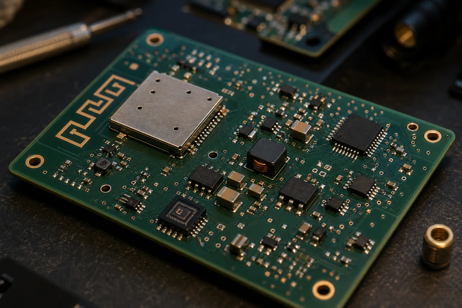
PCB Layout for IoT Devices
PCB layout is where RF performance, power integrity, EMC compliance and DFM requirements intersect. For IoT devices, the RF layout is typically the most critical and most frequently mishandled aspect of the design.
Antenna Design and Keepout Zones
Pre-certified modules carry a keepout zone specification – a copper-free area around the module’s antenna that must be respected on all PCB layers, including inner layers of a multilayer board. Violating this keepout zone degrades the antenna’s radiation efficiency and can invalidate the module’s pre-certification, requiring the product to undergo full radio testing as if the module were not pre-certified. External antennas (PCB trace, chip, wire, or external whip via U.FL connector) each have placement, ground plane and feed line requirements that must be followed for rated performance.
Ground Plane Management
A solid, uninterrupted ground plane on the layer immediately beneath the component layer is the single most important EMC design practice for digital and RF circuits. Cuts, slots or via-fences in the ground plane under high-frequency signal traces or RF components create current return path discontinuities that radiate. Ground plane management also affects the characteristic impedance of microstrip and stripline transmission lines used for controlled-impedance routing of RF, USB and high-speed differential signals.
Power Decoupling
Every digital IC and RF component requires local power decoupling capacitors placed as close as possible to the supply pins. The decoupling capacitor provides a local charge reservoir that supplies fast transient currents without the inductance of the power distribution network. For RF circuits, additional high-frequency decoupling (100 pF to 10 nF ceramic capacitors in parallel) is required to maintain supply rail stability at radio frequencies. Correct decoupling strategy is determined during schematic capture and verified during layout review.
Australian Compliance and Certification
Any IoT device that transmits radio signals and is sold or supplied in Australia must comply with ACMA (Australian Communications and Media Authority) requirements and carry RCM (Regulatory Compliance Mark) certification covering both electromagnetic compatibility (EMC) and electrical safety. For products using pre-certified modules, the compliance path is narrower but not trivial: the supplier’s integration guide must be followed precisely, and the complete product – not just the module – must be assessed for EMC compliance.
Pre-compliance testing during development – conducted in a shielded enclosure or at an accredited test facility – identifies emissions and immunity issues before formal testing. Issues found at this stage typically require layout changes (improved shielding, filter additions, keepout adjustments) that are fast and inexpensive to fix on a prototype. The same issues found at formal certification testing require a board respin, re-testing fees and schedule delay. Zeus Design conducts pre-compliance assessment as part of its IoT device design process and supports clients through formal certification at accredited Australian test houses.
Zeus Design’s IoT Device Design Process
Zeus Design designs IoT hardware as an integrated discipline where hardware architecture, wireless integration, power design and PCB layout are developed by the same team, aligned to the same product requirements. The typical engagement follows these phases:
- Requirements and architecture – wireless protocol selection, power budget modelling, microcontroller or module selection, sensor specification, compliance planning and project scoping. The output is a hardware architecture document that drives all subsequent design decisions.
- Schematic design – full schematic capture covering power supply, microcontroller, radio subsystem, sensor front-end, I/O interfaces and protection circuitry. Design review conducted before proceeding to layout.
- PCB layout – component placement, antenna keepout compliance, controlled-impedance routing, ground plane management, decoupling strategy and DFM review. Layout proceeds in parallel with early firmware development to validate pin assignments and interface specifications before the board is fabricated.
- Prototype fabrication and bring-up – quick-turn PCB fabrication and assembly, systematic board bring-up covering power rails, clocks, communication interfaces and radio link testing. Issues resolved before the design is locked.
- Pre-compliance testing – RF conducted and radiated emissions testing, immunity testing and ACMA compliance assessment. Issues resolved at this stage, before formal certification.
- Production readiness – DFM review, BOM finalisation, assembly documentation, production test specification and test jig development.
Deliverables include Altium PCB design files, schematic PDFs, BOM with approved alternates, assembly drawings, antenna integration documentation, pre-compliance test report and production test specification.
How IoT Device Design Connects to Related Services
The hardware design is one layer of a complete IoT product. Zeus Design’s broader capability covers the full stack:
- Embedded firmware development – Zeus Design’s embedded software development service delivers firmware co-developed with hardware, covering wireless stacks, power management, OTA update, sensor drivers and security features, so that firmware and hardware constraints are resolved before the PCB is finalised.
- Cloud backend and IoT platform integration – device data must go somewhere. Zeus Design’s cloud development practice covers AWS IoT Core and Azure IoT Hub integration, device provisioning, data pipelines, fleet management and OTA update infrastructure.
- Mobile app development – most IoT products require a mobile interface for device pairing, configuration and monitoring. Zeus Design’s mobile app development service covers iOS, Android, BLE and Wi-Fi device pairing, real-time data display and cloud integration.
- Rapid prototyping – for earlier-stage projects where the concept needs validation before committing to a full hardware design cycle, Zeus Design’s rapid prototyping service builds functional proof-of-concept hardware quickly and cost-effectively.
FAQs
What does IoT device design involve?
IoT device design is the hardware-layer discipline covering the architecture and detailed design of the physical connected device. It includes microcontroller or SoC selection, wireless module or radio subsystem design, power supply architecture and battery life modelling, sensor selection and signal conditioning, PCB layout (including antenna integration and RF layout), and compliance planning for ACMA and RCM certification. It is distinct from IoT firmware development and cloud architecture, though all three layers must be designed in coordination.
Which wireless protocol should I use for my IoT device?
The right protocol depends on range requirement, power budget, data rate, deployment environment, infrastructure availability and cost. LoRaWAN is the dominant choice for long-range, battery-powered sensors transmitting small payloads infrequently. LTE-M or NB-IoT suits mobile assets and locations without LoRa infrastructure. Wi-Fi suits mains-powered devices with high throughput requirements. BLE suits short-range applications and direct smartphone pairing. A structured protocol selection process at the start of the project, evaluating the deployment environment and operational requirements, prevents expensive design changes later.
How do I calculate battery life for an IoT device?
Battery life is calculated by modelling the device’s current consumption in each operating state (deep sleep, sensor measurement, radio transmit, radio receive, data processing), weighting each state by its duty cycle, summing to an average current draw, and dividing the battery capacity (in milliamp-hours) by the average current. The model must account for battery self-discharge, temperature effects on capacity, and end-of-life voltage cutoff. This modelling should be completed before schematic design begins, not after the hardware is built.
Do pre-certified wireless modules eliminate the need for compliance testing?
Pre-certified modules (carrying regulatory approval from their manufacturer) simplify the compliance path but do not eliminate it. The module’s integration guide must be followed precisely – particularly antenna keepout zones and recommended layout practices. The complete product, including the module and its surrounding circuitry in the final enclosure, must still be assessed for EMC compliance. Pre-compliance testing during development is strongly recommended to identify integration issues before formal certification testing.
What is the most common reason IoT device designs fail pre-compliance testing?
The most common causes of EMC pre-compliance failures in IoT devices are: antenna keepout zone violations that degrade module radiation efficiency; insufficient power supply decoupling causing conducted emissions on supply pins; ground plane discontinuities under high-frequency signal traces; and inadequate filtering on I/O lines exiting the PCB. All of these are preventable with EMC-aware design practices applied at the schematic and layout stage, before the board is fabricated.
How long does IoT device design take from concept to prototype?
A straightforward IoT device design using a pre-certified module – covering schematic, layout, fabrication, assembly and bring-up – typically takes 8 to 14 weeks. More complex designs involving custom RF circuits, multiple radio protocols, high-channel-count analogue front-ends or challenging mechanical and environmental constraints take 16 to 28 weeks. Pre-compliance testing adds 2 to 4 weeks. Timeline is strongly influenced by how well-defined the requirements are at project start and how many prototype iterations are required.
Can Zeus Design work on an existing IoT hardware design, or do you only do greenfield projects?
Zeus Design regularly engages with teams who have an existing hardware design – a schematic in progress, a prototype with known issues, or a design that has failed pre-compliance testing – and need specialist support to resolve specific problems or take the design to the next stage. Engagements begin with a design review to understand the current state, identify risks and agree on scope. There is no requirement to start from scratch.
Ready to Design Your IoT Device?
Zeus Design works with Australian product teams and hardware startups across the full IoT device design process – from wireless protocol selection and power architecture through PCB layout, RF integration and ACMA compliance. Whether you are starting from a concept or need to resolve issues in an existing design, our electronics design team brings the hardware, RF and power expertise your project needs under one roof.

0 Comments