
Electronics engineering is the discipline that turns a product idea into manufacturable, compliant hardware – and for founders, product managers, and hardware startups evaluating design partners, understanding exactly what an electronics engineering engagement covers is essential before signing a statement of work. This guide breaks down the full scope of electronics engineering services: from schematic capture and signal integrity through to compliance planning, test system development, and embedded firmware, with specific reference to how Zeus Design structures these engagements for Australian and global hardware products.
TL;DR
- Electronics engineering covers the complete hardware development lifecycle – not just PCB layout.
- Key deliverables include schematics, PCB layout, signal integrity analysis, BOM, firmware, and compliance documentation.
- Signal integrity and EMC planning should begin at schematic stage, not after layout.
- Compliance (RCM, CE, FCC) requires design decisions from day one – retrofitting is expensive.
- Test systems (automated test jigs, functional test procedures) are part of engineering, not an afterthought.
- Electronics engineering and embedded software must be developed together for reliable product behaviour.
- Zeus Design delivers end-to-end electronics engineering – hardware, firmware, prototyping, and DFM – under one engagement.
Who This Guide Is For
This post is written for founders and product managers who are either evaluating electronics engineering firms for the first time or who are partway through a product development cycle and need to understand what a professional electronics engineering engagement should include. If you are a non-technical stakeholder trying to ask better questions of your engineering team or supplier, this guide will give you the vocabulary and the framework to do that.
Australian hardware startups in particular face a specific challenge: the local market has a relatively small pool of electronics engineering firms, and the scope of services varies considerably between them. Some firms offer only PCB design; others position themselves as full product development partners. The difference matters enormously for schedule, cost, and certification risk.
What Electronics Engineering Services Include
A professional electronics engineering engagement typically spans several interconnected disciplines. Understanding each one helps you assess whether a proposed scope of work is complete.
Schematic Capture
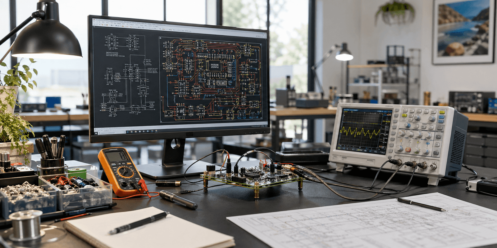
Schematic capture is the process of translating a circuit concept into a formal schematic diagram using electronic design automation (EDA) software – commonly Altium Designer, KiCad, or Cadence. The schematic defines every component, its electrical connections, power rails, reference designators, and the logical structure of the circuit before any physical board layout begins.
A well-structured schematic is hierarchical, annotated, and reviewed against the target application’s electrical requirements. It forms the primary engineering document from which all downstream work – layout, BOM, compliance analysis – derives. Poorly structured schematics are one of the most common sources of board respins.
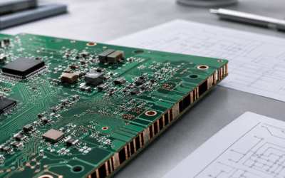
PCB Layout and Signal Integrity
PCB layout translates the schematic into physical copper geometry on a board. For straightforward designs this is relatively mechanical; for high-speed digital, RF, or mixed-signal designs, it becomes a significant engineering discipline in its own right.
Signal integrity (SI) concerns how electrical signals behave as they travel through the board – across traces, vias, connectors, and power planes. At higher frequencies, even small layout decisions (trace length, impedance mismatches, reference plane discontinuities, via stubs) can degrade signal quality, cause timing errors, or generate electromagnetic emissions. SI analysis tools such as HyperLynx or Altium’s built-in simulation environment are used to model and mitigate these effects before the board is manufactured.
Key SI considerations in modern electronics engineering include:
- Controlled-impedance routing for high-speed differential pairs (USB, PCIe, LVDS, Ethernet)
- Return path continuity – maintaining unbroken ground planes beneath high-frequency signals
- Decoupling capacitor placement and power plane design
- Via-in-pad and back-drilling for high-density designs
- Crosstalk and inter-layer coupling management
For detailed PCB layout and design-for-manufacture considerations, Zeus Design’s circuit board design service covers multilayer boards, EMC-aware layout, and production readiness across a wide range of product categories.
Component Selection and BOM Management
Selecting components is an engineering decision, not a purchasing exercise. Component selection affects performance, reliability, cost, supply chain risk, and compliance. A professional electronics engineering firm will maintain awareness of component availability, lead times, lifecycle status (active vs. NRND vs. obsolete), and second-source options.
The Bill of Materials (BOM) produced during design should include manufacturer part numbers, approved alternatives, and sufficient specification headroom to pass qualification testing. Engineering decisions made during component selection have long-term consequences for production cost and supply chain resilience – a lesson many startups learn only after their first production run.
Compliance and Regulatory Planning
In Australia, electronics products placed on the market must meet the Regulatory Compliance Mark (RCM) requirements administered by the Australian Communications and Media Authority (ACMA). Products sold internationally typically also require CE marking (EU) or FCC authorisation (USA), and may need additional certification for specific markets (e.g. UKCA for the UK, MIC for Japan).
Compliance is not a post-design activity – it is an engineering constraint that must be embedded into the design from the outset. EMC (electromagnetic compatibility) design practices, electrical safety (creepage and clearance distances, insulation ratings), and RF module certification requirements all influence schematic and layout decisions. Pre-compliance testing, conducted during prototype stages, is far less expensive than discovering failures at final certification testing.
Standards that commonly apply to Australian electronics products include AS/NZS 4268 (radio communications equipment), IEC 62368-1 (audio/video and IT equipment), and IEC 61010-1 (measurement and control equipment). Engineers Australia notes that compliance engineering requires deep understanding of both the technical standards and the conformity assessment pathways relevant to each product category.
Zeus Design’s electronics design service includes compliance-focused design practices and pre-compliance planning to reduce certification risk and avoid costly redesigns late in the product development cycle.
Embedded Software and Firmware
Modern electronics products are software-defined: the hardware’s behaviour is determined almost entirely by the firmware running on its microcontroller or processor. Electronics engineering and embedded software development must therefore be treated as a single, integrated discipline rather than sequential handoffs between separate teams.
Firmware scope in a typical product engagement includes:
- Hardware abstraction layer (HAL) and peripheral driver development
- Real-time operating system (RTOS) integration where required
- Communication stack implementation (BLE, Wi-Fi, LoRaWAN, LTE-M, CAN, Modbus)
- Bootloader and over-the-air (OTA) update mechanisms
- Power management and low-power sleep modes
- Factory test firmware and production programming procedures
When firmware and hardware engineering are developed in parallel by the same team, hardware bugs are caught earlier, bring-up is faster, and the final product is more reliable. Zeus Design’s embedded software development capability is developed alongside hardware for this reason.
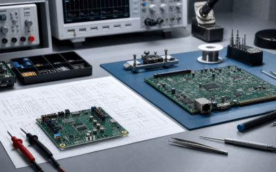
Test System Development
Production test is an engineering function, not a quality control afterthought. For any product manufactured at volume, a functional test system – typically a custom test jig with pogo pin contacts, a control interface, and automated pass/fail logic – is necessary to verify that each unit meets its functional specification before shipping.
Test jig development involves electronics engineering (probe card design, power supply and measurement circuitry), software engineering (test sequencer, data logging, integration with manufacturing execution systems), and mechanical engineering (fixture design, DUT alignment). Designing test systems in parallel with the product design reduces time-to-production and avoids last-minute manufacturing delays.
When a Project Needs Electronics Engineering Expertise
Not every electronics project requires the same depth of engineering. A simple power supply or passive sensor interface requires different expertise than a high-speed FPGA development board or an LTE-M connected medical device. The following signals typically indicate that a project warrants professional electronics engineering engagement:
- High-speed digital interfaces: USB 3.x, PCIe, Gigabit Ethernet, MIPI CSI/DSI, DDR memory – all require SI analysis and controlled-impedance layout.
- RF and wireless connectivity: Antenna design, RF matching networks, conducted and radiated emissions compliance, and co-existence between multiple radio systems require specialist knowledge.
- Safety-critical applications: Industrial, medical, or automotive electronics require rigorous design, documentation, and often formal safety standards (IEC 62443, IEC 60601, ISO 26262).
- Volume production: Any product intended for manufacture at scale needs DFM analysis, test strategy, and supplier qualification built into the design.
- Regulatory certification: Products entering regulated markets require compliance-aware design from the first schematic revision.
- IoT and connected products: Cloud-connected devices add security, firmware update, and backend integration requirements that cross the hardware/software boundary.
Technical Risks and How to Manage Them
Electronics engineering projects fail or overrun for a predictable set of reasons. Understanding these risks allows founders and product managers to structure engagements that mitigate them.
Board Respins
A board respin – manufacturing a revised PCB to fix errors or performance issues from the previous revision – typically costs between $5,000 and $30,000 when prototype manufacturing, assembly, and engineering time are included. Each respin also adds four to eight weeks to the schedule. Most respins are caused by schematic errors, signal integrity issues not caught during review, or compliance failures discovered during testing. Rigorous design review processes and pre-compliance testing reduce respin frequency significantly.
Component Obsolescence and Supply Chain Disruption
The global electronics supply chain has demonstrated its fragility repeatedly in recent years. Engineering decisions made during component selection – choosing parts with multiple approved manufacturers, avoiding single-source components without a clear alternative, designing for component flexibility – have a direct impact on whether a product can be manufactured at volume when it is ready for market.
Firmware-Hardware Integration Failures
When hardware and firmware are developed by separate teams that communicate infrequently, integration failures are common. Hardware features are omitted that firmware assumed would be present; firmware assumptions about timing or electrical behaviour are incorrect; bring-up takes weeks instead of days. Integrated engineering teams – where electronics engineers and firmware engineers work from the same specification – eliminate the majority of these issues.
Late Compliance Discovery
Engaging a compliance test laboratory only at the end of the design process is one of the most expensive mistakes in electronics product development. An EMC failure at final certification testing typically requires a board respin, re-testing, and schedule delays of three to six months. Compliance engineering, beginning at schematic capture, is the correct practice.
Zeus Design’s Electronics Engineering Process and Deliverables
Zeus Design structures electronics engineering engagements around a defined set of phases and deliverables, giving clients visibility into what is produced and reviewed at each stage.
Discovery and Requirements
Every engagement begins with a requirements workshop covering functional specification, target markets and applicable standards, production volume and cost targets, power budget, form factor constraints, and connectivity requirements. This phase produces a written product specification that is agreed before any design work begins.
Concept and Architecture
The architecture phase defines the block-level design: which microcontroller or processor platform, which connectivity stack, which power architecture, and which functional blocks require custom versus off-the-shelf solutions. Architecture decisions made at this stage have a disproportionate influence on the final product’s cost, compliance profile, and firmware complexity.
Schematic Design and Review
Schematic capture is conducted in Altium Designer. Deliverables include hierarchical schematic sheets, a net list, and an initial component BOM with manufacturer part numbers. A formal schematic review is conducted before layout begins, checking for electrical correctness, compliance constraints, and DFM considerations.
PCB Layout and Signal Integrity
Layout follows the schematic review. Controlled-impedance stackup is specified with the PCB manufacturer before layout begins. Signal integrity analysis is performed for high-speed nets. DFM checks are run against the target contract manufacturer’s capabilities. Layout deliverables include Gerber files, drill files, assembly drawings, and a final BOM with approved manufacturers.
Prototype Build and Bring-Up
Zeus Design manages PCB fabrication and assembly through trusted Australian and international contract manufacturers. Prototype bring-up includes power sequencing verification, clock and oscillator checks, communication bus validation, and initial firmware loading. Zeus Design’s rapid prototyping service supports quick-turn builds for early validation and iterative testing.
Firmware Integration and Functional Test
Firmware developed in parallel with hardware is integrated during bring-up. Functional test procedures verify that all hardware features operate correctly. Pre-compliance testing (conducted or radiated emissions, electrical safety) is performed before the final prototype is released.
Design for Manufacture Review and Production Readiness
Before releasing design files for production, a formal DFM review is conducted covering component footprints, solder mask design, assembly panel layout, test point placement, and manufacturing tolerances. Production documentation – assembly drawings, test procedures, packaging specifications – is produced as part of this phase.
How Electronics Engineering Connects to Related Services
Electronics engineering does not exist in isolation. For most hardware products, it interfaces with several adjacent disciplines:
- PCB design and layout – For simpler designs where the engineering scope is primarily layout rather than system architecture, Zeus Design’s circuit board design service provides focused PCB layout and DFM services.
- Embedded software – Firmware and embedded software co-developed with the hardware reduces integration risk and accelerates bring-up. Zeus Design’s software development service covers embedded, desktop, web, and cloud software.
- Rapid prototyping – Early-stage proof-of-concept builds validate feasibility before committing to full electronics engineering. Zeus Design’s rapid prototyping service provides quick-turn functional prototypes for hardware startups.
- Design for manufacture – DFM is embedded throughout the electronics engineering process, not applied at the end. It covers component selection, PCB design rules, assembly processes, and test strategy.
- Compliance and certification – Compliance planning is integrated into electronics engineering from the requirements phase, covering RCM (Australia), CE (EU), FCC (USA), and product-specific standards.
FAQs
What is the difference between electronics engineering and electrical engineering?
Electrical engineering traditionally covers power systems, motors, transformers, and high-voltage infrastructure. Electronics engineering focuses on low-voltage signal processing, semiconductor devices, PCBs, microcontrollers, and consumer or industrial electronics products. In practice, many engineers work across both disciplines, but for product development the relevant discipline is electronics engineering.
How long does an electronics engineering project typically take?
A straightforward product – a single-board microcontroller design with standard interfaces – typically takes eight to sixteen weeks from requirements to first prototype. A complex product with high-speed interfaces, RF, and custom firmware may take six to twelve months. The largest schedule drivers are schematic review cycles, component lead times, and prototype iteration count.
What compliance certifications does my product need in Australia?
Most electronics products sold in Australia require the Regulatory Compliance Mark (RCM), which covers electrical safety and electromagnetic compatibility (EMC). Products with radio transmitters require additional ACMA authorisation. Products exported to Europe need CE marking; those sold in the USA require FCC authorisation. Your electronics engineering firm should advise on the applicable standards during the requirements phase.
When should I involve an electronics engineering firm – at concept stage or later?
As early as possible. Architecture decisions made at concept stage – processor platform, connectivity stack, power architecture, form factor – have an outsized impact on cost, schedule, and compliance. Engaging an electronics engineering firm at concept stage allows these decisions to be made with full engineering awareness rather than retrofitted later at significantly greater cost.
Do I need separate firms for hardware and firmware?
Not necessarily, and often it is better not to. Hardware and firmware are tightly coupled: firmware assumptions drive hardware requirements, and hardware capabilities constrain firmware architecture. When a single team manages both, communication overhead is lower, integration is faster, and technical risk is reduced. Zeus Design develops hardware and firmware together as part of the same engagement.
What does design for manufacture (DFM) mean in practice?
DFM means designing electronics so that they can be reliably assembled, tested, and manufactured at volume without excessive yield loss or rework. Specific practices include correct component footprint tolerances, solder paste stencil design, assembly panel layout, test point placement, and selection of components compatible with automated assembly equipment. DFM review should be conducted before design files are released to a contract manufacturer.
What deliverables should I expect from an electronics engineering engagement?
At minimum: schematic files, PCB layout files (Gerbers, drill files), a finalised BOM with manufacturer part numbers, assembly drawings, test procedures, and a design review report. More comprehensive engagements also include signal integrity analysis reports, pre-compliance test results, firmware source code, and production documentation. Confirm the deliverable list in writing before commencing work.
Working with Zeus Design on Electronics Engineering
Zeus Design is an Australian electronics engineering firm delivering end-to-end hardware product development – from concept and schematic capture through PCB layout, firmware, prototyping, and production readiness. Our engagements are structured for founders and product managers who need a clear scope, defined deliverables, and a technically credible partner who understands both the engineering and the commercial realities of hardware product development.
If you are evaluating electronics engineering services for an upcoming product development project, we are happy to discuss the scope, timeline, and what a well-structured engagement looks like for your specific product.
External references: Engineers Australia – the professional body for engineering in Australia, covering standards of practice and CPD for electronics engineers. IPC Standards – the globally recognised standards body for PCB design and assembly, including IPC-2221 (generic PCB design) and IPC-A-610 (acceptability of electronic assemblies). IEEE – the Institute of Electrical and Electronics Engineers, which publishes foundational standards and research for electronics engineering practice. Standards Australia – the Australian national standards body, publisher of AS/NZS standards applicable to electronics products including AS/NZS 4268 and AS/NZS CISPR series. ACMA – the Australian Communications and Media Authority, responsible for RCM compliance and radio device authorisation.

0 Comments