
PCB design is the discipline that translates an electrical schematic into a manufacturable circuit board, and getting it right the first time is the difference between a smooth production run and costly respins. Whether you are an engineer evaluating design partners, a hardware startup planning your first product, or a product team weighing the cost of bringing PCB layout in-house versus outsourcing, this guide explains every stage of the process – from schematic capture through to Gerber generation – and what to look for in a provider.
TL;DR
- PCB design moves through five stages: schematic capture, component selection, layer stack-up, routing and DFM review.
- Layer count is driven by signal density, power requirements and EMC targets – not just board size.
- The main cost drivers are layer count, board complexity, component density and turnaround time.
- DFM (Design for Manufacture) review catches issues that cause yield loss before the board goes to fab – skipping it is expensive.
- Gerber files, a BOM, assembly drawings and an IPC netlist are the minimum deliverable set for a production-ready design.
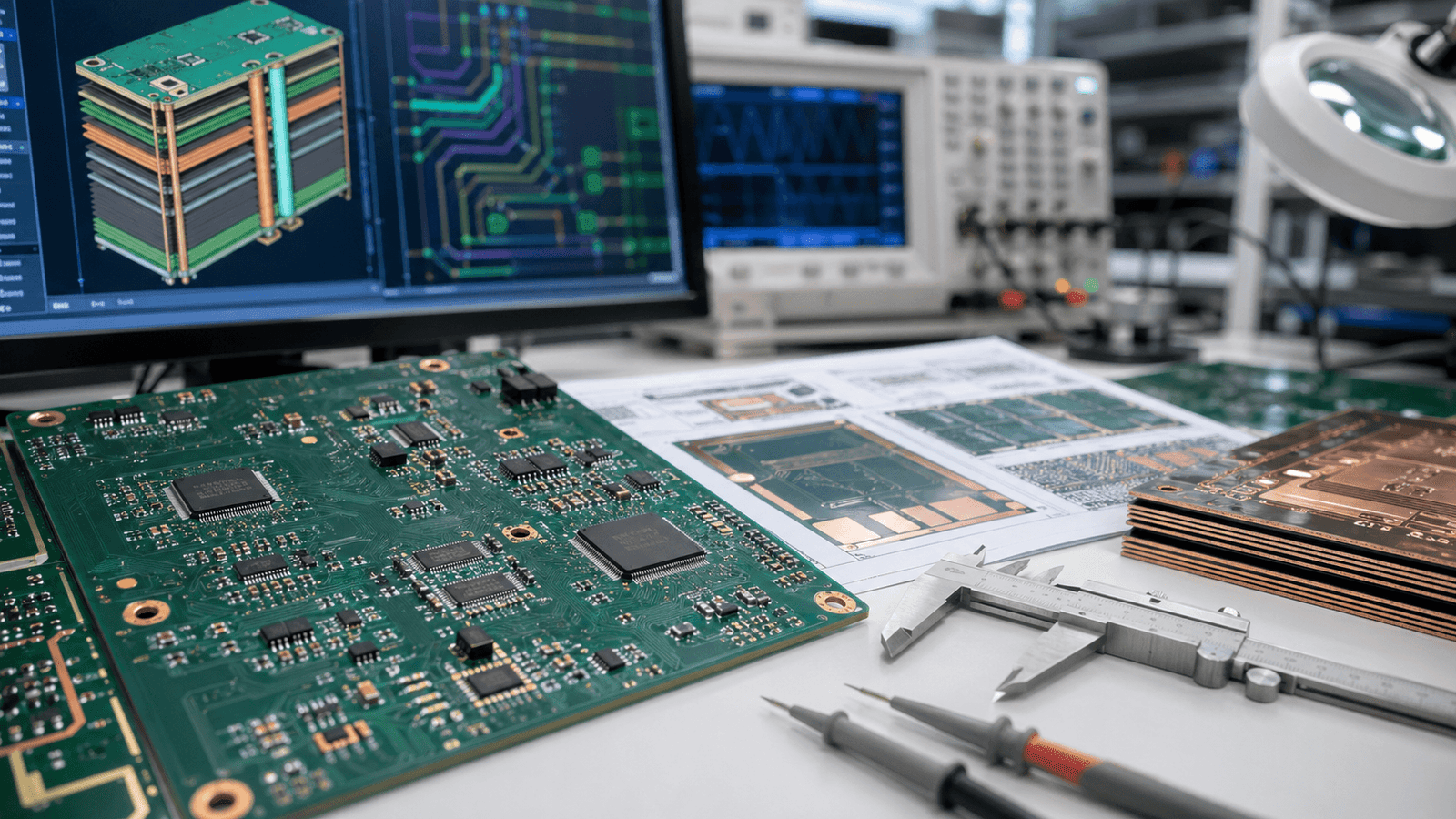
- Zeus Design handles the full PCB design workflow in Altium Designer and delivers files ready for Australian or offshore fabrication.
- PCB layout integrates tightly with firmware and electronics design – treating them as separate engagements adds risk.
Who This Guide Is For
This article is written for engineers, hardware product managers and founders who need to understand what a professional PCB design engagement covers, how decisions made at the layout stage affect cost and yield, and what outputs to expect. It is not a step-by-step layout tutorial – it is a buyer’s guide and technical reference for teams assessing whether to engage a design service such as Zeus Design’s circuit board design service.
What PCB Design Actually Involves
The term “PCB design” is often used loosely to mean just the physical layout, but a complete engagement covers several interconnected phases.
Schematic Capture
Schematic capture is the logical representation of the circuit – components, connections and functional blocks – drawn in EDA (electronic design automation) software such as Altium Designer. A well-structured schematic is hierarchical, clearly annotated and uses net names that survive into the PCB layout. Errors at this stage propagate forward; time spent on a thorough schematic review pays back many times over in avoided layout changes.
Component Selection and Library Management
Component selection is part of the design process, not a separate procurement exercise. Choosing components with appropriate footprints, verified lifecycle status and stock availability at Australian and global distributors prevents last-minute substitutions that require re-layout. Design libraries – footprints, 3D models and simulation models – must match the chosen manufacturer part numbers exactly. Mismatched footprints are one of the most common causes of first-article failures.
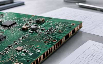
Layer Stack-Up Definition
The layer stack-up defines the physical composition of the PCB: copper layers, prepreg and core materials, and their thicknesses. Stack-up decisions affect impedance control, signal integrity, power delivery, thermal performance and cost. A two-layer board costs significantly less to fabricate than an eight-layer board, but the routing density and signal performance achievable on two layers may be inadequate for the design. Stack-up is agreed between the designer and the fabrication house early in the project – not at the end.
Component Placement
Placement precedes routing and has an outsized influence on the quality of the final design. Good placement groups related circuits, minimises trace lengths for high-speed signals, respects thermal zones around power components, and ensures the board is assembleable – leaving adequate clearance for pick-and-place tooling, soldering processes and test access. Poor placement cannot be rescued by clever routing.
Routing
Routing connects component pins according to the schematic netlist. High-speed differential pairs, controlled-impedance traces, power planes and sensitive analog signals each require different routing strategies. Design rule checks (DRCs) enforce minimum spacing, width and via constraints defined by the fabrication house’s capabilities. Signal integrity simulation tools – including time-domain reflectometry and eye-diagram analysis for high-speed interfaces – are used to validate critical nets before the design is released.
DFM Review
Design for Manufacture review is the systematic check of the completed layout against the tolerances and processes of the intended fabrication and assembly house. It covers minimum annular ring, solder mask expansion, paste aperture ratios, component clearance from board edges and silkscreen conflicts. A DFM pass by an experienced engineer, informed by the IPC-2221 generic standard for printed board design, can eliminate the majority of issues that cause expensive respins or reduced assembly yield.
Gerber Generation and Output Package
The final deliverable set includes Gerber RS-274X or Gerber X2 files for each copper and non-copper layer, an NC drill file, a bill of materials (BOM), assembly drawings, a pick-and-place centroid file, and an IPC-356 netlist for electrical testing. Some fabrication houses also accept ODB++ as an alternative to Gerbers. Providing an incomplete output package is a common source of delays and additional charges from the fab.
Layer Count Decisions: When to Use Multilayer Boards
Layer count is one of the most consequential early decisions in a PCB design project. It directly affects fabrication cost, lead time and design complexity.
Two-Layer Boards
Suitable for simple power supplies, sensor breakouts, low-frequency analogue circuits and cost-sensitive, high-volume consumer products. Component density is limited and there is no dedicated ground plane, which can create EMC challenges for mixed-signal or switching designs.
Four-Layer Boards
The most common configuration for medium-complexity designs. A typical four-layer stack uses two signal layers with dedicated inner ground and power planes. The continuous reference plane significantly improves EMC performance and simplifies routing. Four-layer fabrication costs are roughly 30-60% higher than two-layer at volume but are often justified by the reduction in EMC iteration.
Six and Eight-Layer Boards
Used for high-speed digital designs – processors, FPGAs, DDR memory interfaces, gigabit Ethernet – where multiple dedicated reference planes, controlled impedance and signal shielding are required. Six and eight-layer boards are also common in dense IoT and wireless products where RF, digital and power domains need physical separation.
Ten Layers and Above
Reserved for complex system-on-module (SOM) designs, high-density interconnect (HDI) PCBs, and products with extreme EMC or signal integrity requirements. HDI techniques such as microvias, buried vias and via-in-pad are common at this layer count and require specialist fabrication capabilities.
The IPC-2221B standard provides guidance on design rules, materials and fabrication tolerances applicable across all layer counts. The IPC-A-600 Acceptability of Printed Boards standard defines the visual and dimensional quality criteria used by fabrication houses and incoming inspection teams.
Cost Drivers in PCB Design
Understanding what drives cost allows product teams to make informed trade-offs at the design stage rather than being surprised at quotation time.
Board Complexity and Layer Count
Layer count is the single largest fabrication cost driver. Beyond layers, aspect ratio (board length-to-thickness ratio) affects via drilling cost, and tight impedance tolerances require controlled-impedance laminate testing, adding cost and lead time.
Component Density and Package Types
High component density, fine-pitch BGAs (ball-grid arrays), 01005 passives and other micro-components require more precise assembly equipment, finer solder paste stencils and slower placement speeds – all of which increase assembly cost. They also increase the risk of first-article defects, making pre-production DFM review even more valuable.
Turnaround Time
Standard PCB fabrication lead times from Australian-accessible fabs range from 5-15 business days for standard builds. Expedited services (2-5 days) carry a premium of 30-100% depending on layer count and quantity. Planning lead time into the project schedule is almost always cheaper than paying for expedited turns.
Number of Design Iterations
Each design spin – a re-layout triggered by a functional or DFM issue – adds fabrication cost, assembly cost, engineering time and calendar time. Thorough schematic review, pre-routing simulation for critical signals, and a comprehensive DFM pass before first release are the most effective ways to reduce the expected number of spins.
Compliance Requirements
Designing for regulatory certification (RCM in Australia, CE in Europe, FCC in the US) imposes EMC-aware layout constraints that add design time upfront but avoid costly post-certification redesigns. Pre-compliance testing during the prototype phase allows issues to be caught before the formal submission.
DFM Considerations That Affect Production Yield
Design for Manufacture is not a single check – it is an engineering discipline that spans the entire design process. The following are the DFM issues most commonly encountered in Australian PCB design engagements.
- Insufficient solder mask clearance: Solder mask dams between close-pitch pads that are narrower than the fab’s capability cause bridging during reflow. IPC-7351 land pattern standards provide appropriate pad geometries for common component packages.
- Paste aperture ratio violations: Stencil aperture area-to-volume ratios below 0.66 cause incomplete paste release, resulting in insufficient solder joints – a primary source of field failures in SMT assemblies.
- Via-in-pad without fill and cap: Open vias under BGA pads cause solder wicking during reflow, producing voids and insufficient joints. Filled and capped vias add cost but are required for reliable BGA assembly.
- Tombstoning risk on small passives: Asymmetric thermal loading on 0402 and 0201 resistors and capacitors can cause tombstoning during reflow. Thermal relief connections on these packages need careful evaluation.
- Board edge clearance: Components placed too close to routed board edges are at risk during depanelisation. A 0.5 mm minimum clearance from the rout path is a common fab requirement.
- Test point accessibility: Adequate, accessible test points for in-circuit test (ICT) or flying probe are essential for production test coverage. Designs that omit test points push fault finding to expensive functional test or rework.
The IPC-A-610 Acceptability of Electronic Assemblies standard is the reference used by most Australian contract manufacturers for assembly acceptance criteria and is worth reviewing when specifying quality requirements.
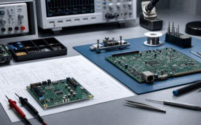
Zeus Design’s PCB Design Process and Deliverables
Zeus Design’s circuit board design service covers the full workflow from schematic capture through to production-ready output files. Designs are completed in Altium Designer, one of the industry’s leading EDA platforms, which provides full schematic-to-layout connectivity, integrated simulation, and direct fabrication output generation.
The engagement typically follows this sequence:
- Requirements review: Functional specification, interface requirements, target layer count, mechanical envelope, regulatory targets and production volume are agreed before design work begins.
- Schematic design and review: Circuit design is completed and reviewed against the functional specification. A formal schematic review with the client is conducted before layout begins.
- Stack-up selection: Layer stack-up is selected in consultation with the intended fabrication house to ensure achievable impedance targets and cost-efficient construction.
- Component placement and routing: Placement is optimised for signal integrity, thermal performance, assembly process and mechanical fit. Routing follows placement with DRC validation at each stage.
- DFM review: Completed layout is reviewed against the fab’s DFM checklist and IPC standards. Issues are resolved before output generation.
- Output package generation: Gerber X2 files, NC drill, BOM, pick-and-place centroid, assembly drawings and IPC-356 netlist are generated and verified against the fabrication house’s file specification.
Clients receive the full native Altium project files alongside the production output package, so the design remains accessible for future revisions without dependency on Zeus Design’s toolchain.
How PCB Design Connects to Related Services
PCB layout does not exist in isolation. The most efficient and lowest-risk product development engagements treat PCB design, electronics design and firmware development as an integrated workflow rather than sequential handoffs between separate teams.
Electronics Design
PCB layout is the physical realisation of the electronic design. When the circuit design and PCB layout are done by the same team – or teams working in close coordination – schematic changes driven by layout constraints (power routing, component placement, decoupling strategy) are handled without costly feedback loops. Zeus Design’s electronics design service covers the full circuit design scope alongside PCB layout.
Rapid Prototyping
Once the PCB design files are complete, moving quickly to a working prototype is the most effective way to validate the design before committing to production tooling and quantities. Zeus Design’s rapid electronics and PCB prototyping service supports quick-turn prototype builds – from bare board procurement through to assembled, tested functional units – that allow design issues to be caught and resolved at low cost.
Firmware and Embedded Software
Hardware and firmware co-development avoids the common failure mode where firmware assumptions about hardware behaviour (interrupt latency, peripheral register behaviour, power sequencing) are not discovered until hardware is on the bench. Starting firmware development against a hardware simulation model or an early prototype, with the PCB design team accessible for clarification, compresses the integration phase significantly.
Compliance and Certification
EMC-aware PCB layout – ground plane continuity, filtering at board entry points, controlled-impedance for clock lines, and RF shielding – is the single most impactful factor in whether a product passes RCM/CE/FCC EMC testing. Compliance planning that starts at the PCB layout stage costs far less than a post-failure redesign.
FAQs
How long does a PCB design project take?
Timeline depends on complexity. A simple two-layer board with fewer than 50 components can be completed in 1-2 weeks. A complex multilayer design with high-speed interfaces, dense BGAs and a full DFM review typically takes 4-8 weeks. Timeline also depends on how quickly schematic review feedback and component approvals are turned around by the client – prompt responses keep projects on schedule.
What is the difference between PCB design and PCB layout?
PCB layout is the physical placement and routing phase of a broader PCB design process that also includes schematic capture, component selection, stack-up definition and DFM review. In common usage, “PCB design” often refers to the full process, while “PCB layout” refers specifically to the placement and routing work in the EDA tool. Most professional engagements cover both.
How many layers does my PCB need?
The minimum layer count is determined by routing density, power delivery requirements and EMC targets. Simple, low-frequency designs are often viable on two layers. Mixed-signal or switching designs almost always benefit from four layers to provide a continuous ground plane. High-speed digital interfaces – USB 3, GigE, PCIe, DDR – typically require six or more layers for adequate signal integrity and EMC performance. Your design partner should be able to make a recommendation based on your schematic and interface requirements.
What files do I need to get my PCB manufactured?
The minimum required for PCB fabrication and assembly includes: Gerber files (one per copper layer, plus solder mask, paste and silkscreen layers), an NC drill file, a BOM with manufacturer part numbers and approved alternates, a pick-and-place centroid file, and assembly drawings. An IPC-356 netlist enables electrical testing at the fabrication stage. Providing an incomplete package is a common cause of delays and additional charges.
What does DFM review involve and why does it matter?
DFM (Design for Manufacture) review checks the completed PCB layout against the fabrication and assembly house’s process tolerances – minimum feature sizes, solder mask clearances, paste aperture ratios, component clearances and via specifications. DFM review catches issues that would cause yield loss or outright assembly failure before the first board is built, making it far less expensive than discovering the same issues during prototype assembly. Most experienced design houses include DFM as a standard step, not an optional add-on.
Can I bring an existing PCB design to Zeus Design for revision or re-layout?
Yes. Zeus Design accepts existing Altium projects, as well as designs in other formats that can be migrated. The usual starting point is a design review to assess the existing schematic and layout against current requirements – this identifies what can be retained, what requires revision, and any DFM issues that need to be resolved before the next production run.
How does PCB design cost compare between Australian and offshore providers?
Offshore PCB design services (India, Eastern Europe, South-East Asia) can offer lower headline rates, but the total cost of a design engagement includes communication overhead, time-zone delays, revision cycles caused by misaligned requirements, and the risk of a design that meets the spec on paper but has not been optimised for the Australian regulatory environment or local assembly capabilities. Australian-based design teams offer direct technical engagement, familiarity with RCM requirements and the ability to work alongside local contract manufacturers – factors that frequently offset the rate differential on projects beyond simple two-layer boards.
Ready to Start Your PCB Design Project?
Zeus Design works with engineers, hardware startups and product teams across Australia on PCB design projects from simple two-layer boards through to complex multilayer designs with high-speed interfaces, wireless connectivity and compliance requirements. Every engagement includes schematic review, full DFM analysis and a complete production output package.

0 Comments