

Choosing the right electronics design services partner is one of the highest-stakes decisions an Australian hardware founder or product manager will make – the wrong choice can cost months of rework, blow out your budget, and delay a market launch. This guide cuts through the noise and gives you a practical framework for evaluating design houses on the criteria that actually matter: end-to-end capability, design for manufacture (DFM), firmware integration, and genuine local support.
TL;DR
- Look for a partner that covers the full product lifecycle – from schematic capture and PCB layout through to firmware, compliance, and DFM – not one that hands off at each stage.
- DFM capability is non-negotiable: design choices made early determine whether your product can be assembled reliably and at scale.
- Firmware and hardware must be developed together – siloed teams create integration debt that surfaces late and expensively.
- Australian-based design houses offer timezone-aligned collaboration, local compliance knowledge (RCM, ACMA), and supply chain continuity advantages.
- Ask for production evidence, not just prototype photos – check whether a partner has taken products all the way to volume manufacture.
- Red flags include: no DFM review step, firmware handled by a separate subcontractor, vague IP ownership terms, and no pre-compliance planning.
- Zeus Design delivers end-to-end electronics design services from Sydney, covering circuit design, PCB layout, embedded firmware, IoT connectivity, and rapid prototyping under one roof.
The Challenge: Why Choosing an Electronics Design Partner Is Hard
The Australian electronics design market ranges from boutique one-person consultancies to mid-size full-service firms, and the differences in capability are not always obvious from a website. Most firms list PCB design and firmware development as services. Far fewer can demonstrate they have integrated hardware, software, and manufacturing considerations from day one – and fewer still have the depth to manage compliance testing and production scale-up.
Hardware founders and product managers face a common trap: selecting a partner based on a compelling initial quote and an impressive prototype, only to discover that the design was never built for manufacture. Respins are expensive. A board that assembles cleanly at 10 units frequently has yield problems at 500 units if DFM has not been treated as a first-class design constraint throughout the project.
The right partner does not just build what you specify – they tell you what you have missed, challenge assumptions early, and structure the work so that moving from prototype to production is a predictable step, not a crisis.
What Electronics Design Services Should Actually Include
A full-service electronics design engagement should cover the following capability areas. Use this as a checklist when evaluating any potential partner:
Circuit and Schematic Design
End-to-end circuit design – analog and digital – optimised for the operating environment, component availability, and cost targets. Schematic review gates should be part of the workflow, not an afterthought.
PCB Layout and Signal Integrity
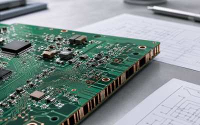
Multilayer PCB layout with attention to impedance control, EMC-aware routing, thermal management, and stack-up selection. Poor layout decisions create EMC failures at pre-compliance that can force complete redesigns. Look for partners using professional toolchains such as Altium Designer for their PCB layout work.
Design for Manufacture (DFM)
DFM analysis should be woven throughout the design process – component footprint verification against manufacturer data sheets, panelisation planning, solder paste stencil optimisation, and assembly constraint checks. Partners who treat DFM as a final sign-off step rather than an ongoing design discipline tend to produce boards that look good on screen but cause assembly headaches in the factory.
Embedded Firmware and Software Integration
Firmware developed in isolation from hardware creates integration risk. The best electronics design partners write firmware in parallel with hardware, so the two are validated together on engineering samples. This is especially critical for real-time control systems, low-power IoT products, and anything with a safety function. Zeus Design’s embedded software development team works alongside hardware engineers throughout the design phase.
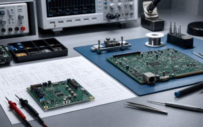
Rapid Prototyping and Proof of Concept
Early-stage validation through quick-turn prototypes – functional PCB assemblies, proof-of-concept builds, and hardware-in-the-loop test setups – reduces downstream risk significantly. A partner who can turn around a working prototype in weeks rather than months keeps your project moving and your options open. See Zeus Design’s rapid prototyping service for the kinds of timelines that are achievable.
IoT Connectivity and Cloud Integration
Connected products require radio design (Wi-Fi, Bluetooth, cellular, LPWAN), antenna placement, RF compliance, and a cloud architecture that can scale. These are not simple bolt-ons – they need to be factored into the hardware architecture from the beginning.
Compliance and Certification Planning
In Australia, most electronic products require RCM marking and ACMA supplier code compliance. Products sold internationally may also need CE, FCC, or UL certification. Pre-compliance planning – designing to the standards before test, running in-house pre-scans – dramatically reduces the cost and delay of formal certification. A design partner who leaves compliance planning until the end of the project is leaving you exposed.
Test Jig and Production Test Development
Repeatability in production depends on having purpose-built test fixtures. A good design partner will develop test jigs alongside the product so that quality control is systematic rather than manual from day one.
Key Evaluation Criteria When Selecting a Design Partner
1. End-to-End Capability or Clear Handoff Plan
The lowest-risk arrangement is a single partner who can carry the project from concept through to production-ready design files. If a partner subcontracts significant portions of the work – particularly firmware or compliance testing – you need to understand exactly who is responsible for integration and who owns the schedule when issues arise at the interfaces between subcontractors.
2. DFM as a Design Discipline, Not a Gate
Ask specifically: at what point does DFM analysis begin? The correct answer is at component selection and footprint review – before layout begins. Partners who treat DFM as a final checklist before releasing Gerbers are likely to produce designs that require assembly process compromises or, worse, board spins driven by manufacturability issues. The IPC standards (IPC-2221, IPC-7711) define baseline expectations for PCB design quality and assembly – ask whether your prospective partner designs to these standards.
3. Firmware Integration Model
Siloed firmware is one of the most common and costly problems in electronics product development. Ask to see the workflow: are hardware and firmware engineers in the same team? Do they share a version-controlled project repository? Is bring-up firmware written before the first prototype is assembled, so validation can begin immediately on receipt of boards? These questions reveal whether a partner treats firmware as part of the product or as an add-on service.
4. Local vs Offshore – What Actually Matters
Offshore design services can appear cost-effective at the quote stage. The true cost of offshore engagement often includes timezone friction (review cycles that span 24+ hours), communication overhead, limited familiarity with Australian compliance requirements, and difficulty conducting in-person design reviews during critical phases. Engineers Australia and AusIndustry’s Industry Growth Programme both emphasise the value of local capability for sovereign hardware development – a consideration that is increasingly relevant for government-adjacent and defence-adjacent products.
A Sydney-based or Australian-based partner can attend factory acceptance tests, participate in supply chain reviews, and respond rapidly when something unexpected happens during production – advantages that are difficult to replicate with offshore arrangements.
5. Track Record and Production Evidence
Prototype capability and production capability are different. Ask for case studies that show products taken all the way to volume manufacture. Ask about yield rates at production scale, about any DFM-driven redesigns the partner has caught before manufacture, and about the longest and most complex project they have delivered. References from previous clients are the most reliable signal of a partner’s real-world capability.
6. IP Ownership and Contract Clarity
Confirm that the design services agreement assigns full IP ownership of all design outputs – schematics, Gerbers, firmware source code, BOMs – to you upon payment. Some design houses retain licences over their own component libraries or firmware frameworks; understand what you are actually receiving and what constraints apply if you change partners in the future.
Red Flags When Evaluating Electronics Design Services
- No DFM review in the quoted scope. If DFM is not explicitly mentioned in the proposal, assume it is not happening systematically.
- Firmware subcontracted to an unnamed third party. Integration problems occur at boundaries – if you cannot meet the firmware team, the integration risk is yours to carry.
- Prototype-only portfolio. A partner who can only show prototypes has not demonstrated the ability to take a product to production.
- No pre-compliance planning. Leaving EMC and regulatory compliance until the end of the design process is a schedule and budget risk.
- Vague IP terms or retained licences on core deliverables. Read the contract carefully – ambiguity here becomes a serious problem if you need to change partners or bring design in-house.
- No test jig in scope. If the proposal does not include production test planning, you will be building quality control from scratch at the factory.
- Single-engineer dependency. Small shops where a single person holds all domain knowledge create delivery risk – illness, departure, or capacity constraints can stall your project with little notice.
Zeus Design’s Approach: What Clients Can Expect
Zeus Design is a Sydney-based electronics design firm that covers the full product lifecycle for Australian hardware founders, startups, and established product companies. The team includes electronics engineers, PCB designers, embedded software developers, and IoT specialists who work as a coordinated unit – not as siloed specialists with separate handoffs.
Every engagement begins with a structured scoping phase that establishes the product requirements, operating environment, compliance obligations, and target production volume before design work begins. DFM constraints are introduced at schematic stage and maintained through layout, not reviewed as a final gate. Firmware is developed in parallel with hardware, with bring-up validation conducted on the first engineering samples.
Zeus Design’s pre-compliance approach – designing to IPC and relevant Australian and international standards from the outset – significantly reduces the risk of late-stage surprises during formal certification. The team has experience with RCM, CE, FCC, and other major regulatory frameworks, and can advise on the most efficient path to market for your specific product and target regions.
For clients at the early stage, Zeus Design’s rapid prototyping capability provides a fast path to a working proof of concept that can be used for investor demonstrations, market validation, and early user testing – without committing to a full production design prematurely. CSIRO’s advanced manufacturing resources and the broader Australian innovation ecosystem provide a strong context for this kind of early-stage hardware development.
How Zeus Design’s Services Connect
One of the most important things to understand about choosing an electronics design partner is how the different service areas interact. These are not independent offerings – they are deeply coupled, and the value of a full-service partner comes from managing those couplings well.
Circuit board design sets the foundation: the schematic determines component selection, cost, power architecture, and signal integrity. Every downstream decision – layout, firmware, compliance, test – is constrained by decisions made at schematic stage. Zeus Design’s circuit board design and PCB layout service is built around getting these foundational decisions right, with structured design reviews at schematic and layout stages.
Rapid prototyping translates the design into a working physical system as quickly as possible. The goal is not just to have a board – it is to have a platform for firmware bring-up, functional testing, and early validation. When prototyping is managed as part of the same engagement as design, the team can respond immediately when something unexpected surfaces in the first build.
Embedded software and IoT connectivity are increasingly where product differentiation lives. A connected sensor node or industrial IoT gateway is only as good as its firmware, its communication stack, and its cloud integration. Zeus Design develops embedded software and IoT architecture alongside hardware – ensuring that the firmware is written to the hardware that actually exists, and that the hardware is designed to support the software requirements that have been identified.
When these three service areas are managed by a single coordinated team, the result is a product that is coherent across all layers – electronic, mechanical, software, and connectivity – and that is ready for manufacture without the redesign cycles that typically arise when services are sourced from separate vendors. Standards Australia’s electrotechnology standards catalogue provides the regulatory baseline that governs Australian electronics product requirements.
FAQs
What do electronics design services typically include?
A full-service engagement covers circuit schematic design, PCB layout, embedded firmware development, IoT connectivity, design for manufacture (DFM), compliance planning, rapid prototyping, and test jig development. The best partners manage all of these as a connected workflow rather than separate deliverables handed off between teams or subcontractors.
How do I evaluate a design house’s DFM capability?
Ask at what stage DFM analysis begins – the correct answer is component selection and footprint review, before PCB layout. Ask for examples of DFM-driven changes made during a project and what issues were caught before manufacture. Request that the proposal explicitly includes DFM review as a named deliverable, not an implied activity.
Should I choose a local Australian design partner or go offshore?
Local partners offer timezone-aligned collaboration, knowledge of Australian compliance requirements (RCM, ACMA), and the ability to participate in factory and supply chain reviews in person. Offshore arrangements can introduce timezone friction, communication overhead, and compliance gaps that erode the apparent cost savings over the course of a project.
Why does firmware need to be developed alongside hardware?
Hardware and firmware are deeply interdependent. Firmware written to a specification rather than to real hardware frequently encounters register-level differences, timing dependencies, and peripheral quirks that require hardware changes. Developing both together – with early bring-up firmware validated on the first engineering samples – surfaces these issues when they are cheapest to resolve.
What questions should I ask about IP ownership?
Confirm that all design deliverables – schematics, Gerbers, firmware source code, BOMs, test scripts – are assigned to you upon payment with no retained licences. Ask whether the partner uses any proprietary frameworks or component libraries in the design, and what your rights are with respect to those elements if you need to change partners or bring the design in-house.
How long does a typical electronics design project take?
A straightforward connected product – single-board design, simple firmware, standard connectivity – might reach a production-ready design in three to six months. Complex, multi-board systems with custom RF, safety functions, or extensive certification requirements can take twelve to eighteen months. Early-stage proof-of-concept builds can often be completed in four to eight weeks. Timeline is heavily influenced by requirements stability and how quickly design review feedback is turned around.
How does Zeus Design handle compliance and certification?
Zeus Design builds compliance planning into the design from the beginning – identifying applicable standards (RCM, CE, FCC, and others depending on target markets) at scoping stage, designing to those standards throughout, and conducting pre-compliance checks before formal testing. This approach reduces the risk of certification failures and redesigns that arise when compliance is treated as an end-of-project activity.
Choosing the Right Electronics Design Partner
The decision comes down to three things: capability breadth, integration model, and track record. A partner who covers circuit design, PCB layout, embedded firmware, and DFM under one roof – and who has done it for products that reached volume production – eliminates the coordination overhead and integration risk that arise when services are sourced separately. For Australian hardware founders and product managers, the added advantages of local compliance knowledge, timezone-aligned collaboration, and the ability to engage in person during critical project phases make a strong case for choosing a local, full-service design house.
Zeus Design works with Australian hardware founders, startups, and established product companies to deliver electronics design services that cover the full product lifecycle – from first concept to production-ready design. If you have a product to build, the conversation starts here.

0 Comments