
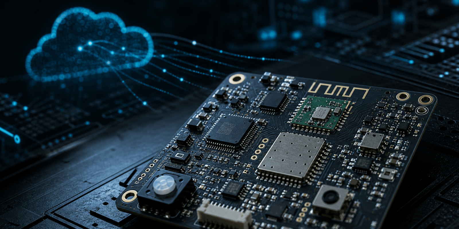
IoT product design services cover a wider scope than most product teams expect – hardware architecture, embedded firmware, wireless connectivity, mobile app development and cloud backend integration all need to work together before a connected device is ready to ship. This guide is for founders, product owners and engineering managers evaluating what a capable IoT product design partner should deliver across the full development process, from initial concept through to a production-ready connected product.
TL;DR
- IoT product design services span five layers: hardware, firmware, wireless connectivity, mobile app and cloud backend – gaps between any of these layers are where most project failures occur.
- Hardware decisions made early constrain everything that follows – MCU selection, power architecture, sensor interfaces and RF layout all affect firmware capability, wireless performance and compliance path.
- Wireless protocol selection (Wi-Fi, BLE, cellular, LPWAN) should be driven by power budget, data rate, range and deployment environment, not convenience.
- Firmware and hardware must be co-designed – treating them as sequential workstreams is one of the most common causes of schedule overruns and board respins.
- The mobile app and cloud backend need to be designed around the device’s data model and communication patterns from the start, not retrofitted after hardware ships.
- An integrated IoT design partner eliminates the handoff gaps between hardware, firmware and software teams that cause the most expensive IoT project failures.
- Simple IoT products typically take 3-6 months; industrial or multi-device deployments commonly run 12-18 months. Planning for integration time is as important as planning for build time.
Why IoT Product Development Is More Complex Than It Appears
A connected device looks simple from the outside: a sensor reads data, firmware processes it, the device transmits it wirelessly, and a cloud backend stores and surfaces it through a mobile app. In practice, most IoT products that run into serious trouble do so at the integration points – where hardware meets firmware, where firmware meets wireless, and where the device protocol meets the cloud.
The engineering disciplines involved in a complete IoT product are genuinely distinct. A hardware engineer optimising for power efficiency, RF layout and compliance is working in a different domain from a firmware engineer writing a real-time sensor acquisition loop and an MQTT stack, who is in turn working differently from a cloud architect designing device management APIs and time-series data pipelines. When these disciplines are siloed across different contractors or internal teams without clear interface definitions, integration cost grows quickly and redesign risk rises sharply.
According to Intuz’s IoT Product Development Guide (2026), simple IoT solutions typically take 3-6 months to design, build and test, while industrial platforms and complex multi-device deployments commonly require 12-18 months. Those estimates assume competent integration across all layers. Projects that treat hardware and software as separate workstreams routinely run longer and cost more to correct.
For Australian product companies – hardware startups, industrial businesses, medtech teams and B2B product owners – this integration question is the core reason to evaluate IoT product design services carefully. The question is not whether a partner can do hardware or software, but whether they can deliver a coherent product across all five layers of a connected device.
What IoT Product Design Services Should Cover
A complete IoT product design service addresses five layers. Here is what each involves and why it matters to the overall product outcome.
1. Hardware Architecture and PCB Design
Hardware is the foundation of every IoT product. Decisions made at this layer constrain what is possible in firmware, which wireless protocols are viable, what the power budget looks like, and what the compliance path will cost. Competent IoT hardware design requires:
- Microcontroller or microprocessor selection – matched to compute requirements, peripheral interfaces, power envelope, wireless support and long-term component availability. An industrial asset tracker, a consumer wearable and a smart meter all have different MCU requirements.
- Power architecture – battery-operated IoT devices need careful power management across sleep modes, regulator efficiency and peak current during wireless transmission. A poorly designed power subsystem will drain batteries faster than specified and generate field failures.
- Sensor and peripheral integration – each sensor interface (I2C, SPI, UART, ADC) requires careful routing, decoupling and layout. Signal integrity issues at the hardware level show up later as intermittent firmware bugs that are expensive to diagnose.
- RF layout and antenna design – wireless module placement, ground plane geometry and antenna routing have a direct impact on link budget and range. Many first-time IoT PCBs underperform in the field because RF layout was treated as an afterthought rather than a design constraint.
- Compliance planning – designing for regulatory certification (ACMA/RCM in Australia, FCC, CE in export markets) from the start reduces the risk of costly hardware respins late in the project. This includes EMC-aware layout and selecting certified wireless modules where appropriate.
Zeus Design’s electronics design service covers hardware architecture, schematic design, PCB layout and compliance planning as an integrated capability, not a series of separate handoffs.
2. Embedded Firmware Development
Firmware is the software that runs directly on the device’s microcontroller. It defines what the device does, how it manages power, how it acquires sensor data and how it communicates wirelessly. Firmware quality determines field reliability more than any other single factor.
Key elements of IoT firmware development include:
- Hardware abstraction and driver development – firmware must be written against the specific peripheral configuration of the PCB. Drivers for sensors, wireless modules, displays and storage need to be developed and validated against the actual hardware, not generic reference designs.
- Real-time operating system (RTOS) or bare-metal design – the choice between an RTOS (such as FreeRTOS or Zephyr) and a bare-metal loop depends on task complexity, timing requirements and memory constraints. This decision has long-term maintainability implications.
- Power management firmware – managing sleep states, wake events and radio duty cycling in firmware is critical for battery life. This requires close coordination with hardware design, particularly around wake-up circuitry and interrupt handling.
- OTA (over-the-air) update capability – field-deployable IoT products need a secure, reliable mechanism to receive firmware updates. Building this in from the start is significantly easier than retrofitting it after initial release.
- Security implementation – secure boot, encrypted storage and authenticated communication channels need to be designed into firmware architecture, not added later. The OWASP IoT Security Project provides a practical framework for understanding the attack surface of connected devices.
Zeus Design develops embedded firmware within the same engagement as hardware design. Firmware architecture is informed by the PCB design and vice versa – the most common source of IoT integration failures is eliminated by default.
3. Wireless Connectivity Design
Selecting the right wireless protocol is one of the most consequential decisions in an IoT product, and it is rarely obvious. The main options each involve genuine trade-offs:
| Protocol | Best for | Trade-offs |
|---|---|---|
| Wi-Fi (802.11) | High data rate, fixed location devices, home/office deployment | High power consumption, requires existing infrastructure |
| Bluetooth Low Energy (BLE) | Wearables, proximity sensing, short-range mobile app pairing | Limited range, point-to-point topology complexity at scale |
| Cellular (LTE-M / NB-IoT) | Mobile assets, remote deployments, wide-area coverage | Ongoing data costs, module cost, power higher than LPWAN |
| LoRaWAN / LPWAN | Long range, low data rate, battery-operated field devices | Very low data rate, latency, network coverage dependency |
| Thread / Zigbee / Matter | Smart home mesh, local automation, low latency control | Gateway/hub dependency, ecosystem compatibility considerations |
Protocol selection should be driven by power budget, data rate, range, deployment environment and long-term network availability – not by familiarity or convenience. The Australian Radio Communications and Media Authority (ACMA) requires devices transmitting in licence-exempt bands to meet specific technical standards; selecting certified modules and understanding the regulatory requirements early avoids compliance surprises. Refer to the ACMA RCM user guide for Australian regulatory compliance obligations.
4. Mobile App Development
For most consumer and prosumer IoT products, the mobile app is the primary user interface – how the end user configures the device, monitors data and controls behaviour. It is also a common source of project delays when scoped and started too late.
IoT mobile app development involves specific considerations that standard app development does not:
- Device pairing and provisioning – onboarding a user’s device to their account, connecting it to Wi-Fi or associating it via BLE, needs to be a reliable and smooth user experience. This is where many IoT apps fail in early user testing.
- Real-time data display and control – IoT apps typically need to display live sensor readings, send commands to devices and handle connectivity interruptions gracefully. This requires thoughtful state management and error handling.
- Push notifications and alerts – threshold alerts and status notifications are often a core feature; implementing these through the cloud backend to push notification infrastructure requires coordination across app, cloud and firmware layers.
- Cross-platform delivery – most IoT product teams need both iOS and Android coverage. Cross-platform frameworks like React Native or Flutter provide an efficient path when the app’s hardware interaction requirements (BLE, Wi-Fi provisioning) are within their native module capabilities.
Zeus Design’s mobile app development service covers iOS, Android and cross-platform development with specific capability in IoT integration – BLE pairing, device provisioning, real-time data display and cloud API integration.
5. Cloud Backend and Data Architecture
The cloud backend receives data from IoT devices, stores it, processes it and serves it to applications and users. IoT cloud architecture differs from standard web application backends in ways that matter to the overall system design:
- Device authentication and identity management – each device needs a unique cryptographic identity that allows the backend to authenticate it without human intervention. X.509 certificates or pre-shared keys at scale require a provisioning workflow that starts in manufacturing.
- MQTT / AMQP messaging – IoT devices typically communicate over lightweight messaging protocols rather than standard HTTP. AWS IoT Core, Azure IoT Hub and similar services manage this at scale; selecting and configuring the right broker is an architectural decision with long-term implications.
- Time-series data storage – IoT devices generate time-stamped measurement data at regular intervals. Relational databases are a poor fit; time-series databases (InfluxDB, TimescaleDB, AWS Timestream) or cloud-native IoT data services are more appropriate and more cost-efficient at scale.
- OTA update pipeline – the backend needs to manage firmware version state, stage rollouts, handle failed updates and provide rollback capability. This is an operational concern that needs architectural support from day one.
- API design for mobile and web clients – REST or GraphQL APIs that serve the mobile app need to be designed around the app’s data requirements and the device’s data model, with appropriate authentication (OAuth2/JWT) and rate limiting.
Zeus Design’s cloud development service covers IoT backend architecture, device management APIs, time-series data pipelines and cloud-connected software systems.
When a Product Needs Integrated IoT Product Design Services
Not every hardware project needs the full stack. A product using an existing certified wireless module and a standard cloud platform may assemble a competent team from specialist contractors with careful interface specification. But integrated IoT product design services become the lower-risk choice when:
- The product involves custom hardware – a new PCB rather than a dev board – where firmware is being developed alongside electronics
- The wireless connectivity is a performance-critical part of the product, not just a standard add-on
- The mobile app is a primary user interface, not a secondary monitoring tool
- The cloud backend needs to handle data from many devices, manage device identity, or support OTA updates at scale
- The project timeline is constrained and parallel workstreams across hardware, firmware, app and cloud need active coordination
- Regulatory certification (RCM/ACMA, CE, FCC) is on the critical path and compliance design needs to start at the hardware stage
The most expensive IoT project failures are not usually failures of individual disciplines – they are failures at the handoffs between disciplines. An integrated partner eliminates the most costly category of IoT project risk by design.
Technical and Commercial Risks to Manage
IoT product development carries a specific risk profile worth understanding before committing to an approach:
Hardware Respins
A hardware revision (board respin) typically costs $15,000-$50,000+ in engineering time, component procurement and revised PCB fabrication, and adds 6-12 weeks to the schedule. The most common causes are RF layout issues discovered during field testing, power management problems found during battery life testing, and signal integrity issues that appear as intermittent firmware bugs. Pre-compliance RF testing and design review before fabrication are worth the investment.
Wireless Performance Gaps
IoT products frequently underperform their wireless range specifications in real-world deployments. Lab performance is measured under ideal conditions; field deployments involve walls, metal enclosures, interference and multipath effects. Range testing in realistic conditions should be scheduled before design lock, not after.
Security Architecture Gaps
IoT security that is retrofitted after hardware design is locked is expensive and usually incomplete. Secure boot requires hardware support (a root of trust, typically in the MCU or a secure element). Encrypted communication requires firmware memory budget. Device identity management requires a provisioning workflow that spans manufacturing and cloud onboarding. These cannot be added cleanly after the fact – they need to be designed in from the start.
Cloud Scaling Surprises
Cloud infrastructure that works well for 100 devices can fail under the load patterns of 10,000. IoT traffic has distinct characteristics – many connections maintained simultaneously, bursty data at scheduled intervals, and high fan-out for OTA updates – that differ from standard web traffic. Architecting for scale from the beginning is cheaper than re-architecting under production load.
The Zeus Design IoT Product Development Process
Zeus Design delivers IoT product design services as an integrated engagement covering hardware, firmware, wireless, mobile and cloud. The team that designs the PCB works directly with the team writing firmware and the team building the app and backend – there are no handoff gaps to manage.
A typical project engagement follows this sequence:
- Architecture and feasibility – define the system architecture across all five layers, identify the highest-risk decisions, establish the wireless protocol, cloud platform and app framework choices, and produce a realistic project plan.
- Hardware design and prototyping – schematic capture, PCB layout with RF-aware design, BOM selection and first-article PCB fabrication. Zeus Design’s rapid prototyping service supports quick-turn first boards for early firmware bring-up.
- Firmware bring-up and integration – peripheral driver development, RTOS integration, sensor validation and wireless stack integration, running in parallel with hardware prototyping where possible.
- Cloud and mobile development – backend device management infrastructure, data pipelines, mobile app development, API integration and end-to-end system testing.
- Compliance and pre-production – pre-compliance RF testing, EMC assessment, DFM review, test jig development for production validation, and handover to contract manufacturing with production-ready documentation.
How IoT Product Design Connects to Related Services
An IoT product is rarely a standalone electronics project. The development process typically draws on a broader set of capabilities that need to stay coordinated:
- Electronics design and PCB layout – the hardware foundation; covers circuit design, schematic capture, PCB layout, DFM and compliance planning
- Embedded software development – firmware, RTOS integration, hardware abstraction, power management and OTA update capability
- IoT connectivity – wireless protocol selection, antenna design, certified module integration and connectivity validation
- Mobile app development – iOS and Android app development with BLE/Wi-Fi pairing, real-time data display and cloud API integration
- Cloud development – IoT backend infrastructure, device management, time-series data storage and APIs
- Rapid prototyping – quick-turn PCB builds for early validation and firmware bring-up
- Test jig development – production test fixtures for repeatable validation of IoT hardware at volume
Zeus Design covers all of these capabilities within a single engagement. Interface definitions between layers are managed internally, not negotiated across contractor boundaries.
FAQs
What do IoT product design services typically include?
IoT product design services cover hardware architecture and PCB design, embedded firmware development, wireless connectivity design and integration, mobile app development, and cloud backend infrastructure. A full-service provider handles all five layers as an integrated engagement rather than as separate specialist contracts, which eliminates the most common category of IoT project failures – integration gaps between disciplines.
How long does it take to develop an IoT product from concept to production?
Simple IoT products with standard wireless connectivity and a straightforward cloud backend typically take 3-6 months from concept to first working prototype, with a further 2-4 months for compliance, DFM and production ramp-up. More complex products involving custom hardware, multi-protocol connectivity, industrial compliance or large-scale device management commonly take 12-18 months end to end. Timeline estimation should account for integration and testing time, not just build time.
What is the difference between IoT product design services and standard electronics design?
Standard electronics design covers hardware architecture, PCB design and often firmware. IoT product design services extend this to include wireless connectivity design, cloud backend development and mobile or web application development – the additional layers required to make a device connected and useful to an end user. The integration between these layers is where most IoT-specific project complexity lives.
Which wireless protocol should I choose for my IoT product?
Protocol selection depends on power budget, data rate requirements, range, deployment environment and network infrastructure. Wi-Fi suits fixed, data-intensive devices; BLE suits short-range pairing and wearables; cellular (LTE-M/NB-IoT) suits mobile or remote assets needing wide-area coverage; LoRaWAN suits long-range, low-data-rate field devices. Zeus Design’s electronics design and IoT connectivity service includes protocol selection as part of the architecture phase.
How important is security in IoT product design?
Security is foundational, not optional. IoT devices are persistent, networked endpoints with physical access in many deployment environments – they present a different attack surface from web applications. Secure boot, encrypted communications, device identity management and OTA update security need to be designed in from the hardware and firmware stages. Retrofitting security after hardware is locked is expensive and typically incomplete. The OWASP IoT Security Project outlines the key attack vectors to design against.
Can Zeus Design handle both the hardware and software sides of an IoT product?
Yes. Zeus Design delivers IoT product design as an integrated service covering hardware architecture, PCB design, embedded firmware, wireless connectivity, mobile app development and cloud backend – the same team coordinates across all layers rather than managing separate contractors. This structure is specifically designed to eliminate the handoff gaps between hardware and software disciplines that cause the most expensive IoT project failures.
What should I prepare before engaging an IoT product design partner?
A clear product brief covering intended use cases, target user, deployment environment, wireless connectivity requirements, required battery life or power source, approximate production volume and any known regulatory markets is enough to start a productive architecture conversation. You do not need detailed technical specifications at the start – establishing those is part of the architecture phase. Zeus Design can work from a product concept and business requirements to produce an initial system architecture and project plan.
Conclusion
IoT product design services span a wider scope than any single engineering discipline – hardware, firmware, wireless connectivity, mobile app and cloud backend all need to work together, and gaps between layers are where most connected product projects run into trouble. Choosing an integrated IoT design partner rather than assembling specialist contractors is a risk management decision: integration is where cost and schedule overruns accumulate, and it is where a well-structured partner delivers the most value.
For Australian product companies building connected devices – a smart industrial sensor, a consumer wearable, a building management node, a B2B field device – the architecture decisions made at the start of the project determine what is achievable, how long it takes and what it costs to fix problems. Getting the architecture right across all five layers, and maintaining coherence between them throughout development, is the core capability that a quality IoT product design service delivers.
Zeus Design provides integrated IoT product design services covering electronics hardware, embedded firmware, wireless connectivity, mobile app development and cloud backend. If you are scoping an IoT product and want to understand what the development process looks like for your specific requirements, get in touch with the Zeus Design team.
")


0 Comments