
Electronic product design is the process of turning a hardware concept into a validated, manufacturable device – and for product teams, founders and hardware startups in 2026, knowing what each phase demands is the difference between a smooth launch and a costly redesign. This guide covers the full lifecycle: feasibility and concept work, PCB design, firmware development, regulatory compliance and production handover, with practical notes on where an integrated partner like Zeus Design fits into each stage.
TL;DR
- Electronic product design spans six key phases: feasibility, concept and architecture, PCB and circuit design, firmware and software, compliance and validation, and production handover.
- Skipping or compressing early phases – especially feasibility and design-for-manufacture (DFM) reviews – is the most common driver of late-stage cost blowouts.
- Firmware and hardware design must be developed in parallel; late firmware integration is a major source of schedule slippage.
- Compliance (EMC, RCM, CE/FCC) needs to be designed in from the start, not bolted on before certification testing.
- A full-service partner covering electronics design, PCB layout, firmware, prototyping and software avoids the coordination risk of managing multiple specialist contractors.
- Zeus Design handles end-to-end electronic product development for Australian product teams, from concept through to production-ready deliverables.
Who This Guide Is For
This guide is for product owners, startup founders, engineering managers and industrial businesses planning or running a hardware development project. Whether you are mapping out a first product or trying to understand where risk is accumulating mid-project, the goal is the same: give you an accurate picture of what electronic product design involves, where projects stall, and how a well-structured development partner keeps things moving.
If you have an in-house electronics team, this guide is also a useful reference for scoping external support – for example, bringing in specialist PCB layout, firmware or compliance expertise for specific phases while keeping architecture decisions in-house.
Phase 1: Feasibility and Requirements
Every electronic product design project begins with a feasibility assessment, whether it is formalised or not. The central questions are: can this be built with current technology, at an acceptable cost, within the available timeline – and what are the key technical risks?
Feasibility work typically covers:
- Functional requirements: What must the product do? Define inputs, outputs, interfaces, connectivity, power budget, form factor and environmental conditions.
- Component availability: Are the key semiconductors and modules available, and what is the lead time? Supply chain risk is a real design constraint in 2026, not a procurement afterthought.
- Regulatory landscape: Which markets will the product enter? RCM (Australia), CE (Europe) and FCC (US) all have different requirements, and some product categories – medical, industrial, safety-critical – carry additional obligations.
- Cost targets: What is the acceptable BOM cost at target production volume? This shapes component selection decisions made throughout the design phase.
- Development budget and timeline: What is realistic given the complexity of the design and the maturity of the concept?
Projects that skip feasibility work tend to hit the same wall: a component on 52-week lead time, a form factor that cannot pass EMC without a board re-spin, or a BOM cost that does not work at target volume. Catching these at the planning stage costs hours. Catching them at prototype review costs months.
Zeus Design’s electronics design service includes feasibility assessment as part of the initial project scoping phase. This gives product teams a clear risk register and realistic project plan before committing to full development.
Phase 2: Concept Design and System Architecture
With requirements defined and feasibility confirmed, the next phase is concept design – translating requirements into a technical architecture. This is where major decisions are made that affect every subsequent phase.
Key decisions in this phase include:
- Microcontroller or processor selection: MCU vs SoC vs module, clock speed, memory, peripheral set, operating voltage and power consumption profile.
- Connectivity architecture: Wi-Fi, Bluetooth, cellular (LTE-M, NB-IoT), LoRa, Zigbee – or wired interfaces like Ethernet, CAN or RS-485. Each has different power, cost, certification and reliability trade-offs.
- Power architecture: Battery chemistry, charge management, power rail sequencing, sleep modes and thermal budget.
- Software and firmware architecture: RTOS vs bare-metal, communication stack, OTA update capability, security model and cloud connectivity approach.
- Mechanical integration: PCB form factor, connector placement, thermal management and enclosure constraints.
Architecture decisions are hard to reverse. A microcontroller chosen for cost that cannot meet interrupt latency requirements, or a wireless module selected without factoring in certification costs, will derail the project at a later and more expensive stage. Getting these decisions right the first time is the primary job of this phase.
For IoT and connected products, Zeus Design’s IoT connectivity and electronics design capability covers the full architecture decision set, including wireless module selection, cloud connectivity design and security architecture.
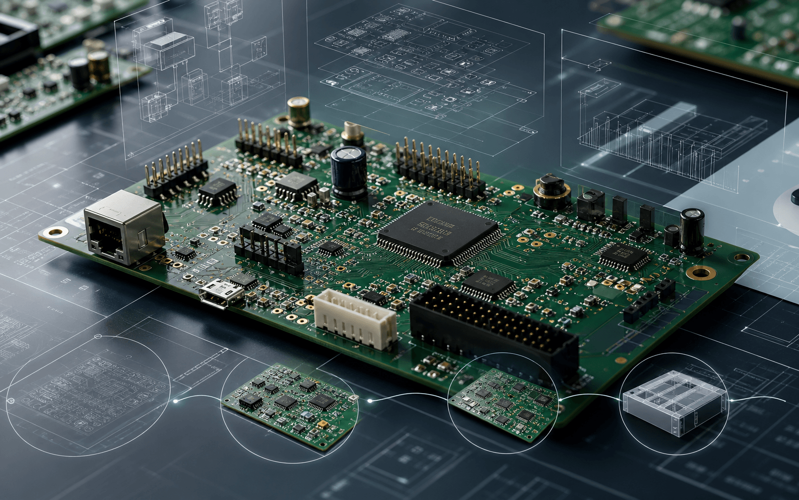
Phase 3: PCB Design and Circuit Development
PCB design is the technical heart of electronic product design. It translates the schematic – the logical description of how components connect – into a physical layout that can be manufactured reliably.
A production-quality PCB design process covers:
- Schematic capture: Precise documentation of every component, net and interface. Errors at schematic stage propagate through to layout and firmware – rigorous schematic review is essential before layout begins.
- Component selection and BOM management: Part selection for performance, availability, cost and thermal characteristics. Approved alternates should be identified at design time, not when a primary component goes on allocation.
- PCB layout: Component placement, layer stack-up, trace routing, controlled impedance for high-speed signals, power and ground plane design, and thermal management. EMC-aware layout – keeping noisy digital signals away from sensitive analogue and RF sections – is fundamental, not optional.
- Design Rules Check (DRC): Automated verification against manufacturer design rules and internal standards before Gerbers are generated.
- DFM review: Design-for-manufacture checks confirm that the board can be assembled reliably and cost-effectively at the target production volume. Altium’s DFM/DFA guidance outlines how these checks integrate into a systems engineering workflow.
Zeus Design uses Altium Designer for PCB layout and applies DFM review as a standard part of the design process, not an afterthought. The circuit board design service covers schematics, multilayer PCB layout, signal integrity, EMC-aware design and production readiness.
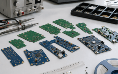
Phase 4: Rapid Prototyping and Validation
No matter how rigorous the design process, a first-article prototype will surface issues. The goal of rapid prototyping is to discover and resolve those issues quickly and cheaply – before tooling, before certification testing, and well before production.
A structured prototyping sequence typically runs:
- Proof of concept (PoC): Often uses development boards and off-the-shelf modules to validate the core technical approach. Quick to build, quick to test. The objective is de-risking the fundamental architecture before committing to custom PCB design.
- Prototype v1 (engineering prototype): Custom PCB with production-intent schematic. Used to validate circuit performance, firmware integration, power management and mechanical fit. Functional but not necessarily at production cost or form factor.
- Prototype v2 (design validation): Incorporates lessons from v1. Closer to production intent in terms of component selection, form factor and manufacturing process. Used for pre-compliance EMC testing and user testing where applicable.
- Pre-production pilot: Small run (typically 5-50 units) built using the intended production process and supply chain. Validates assembly instructions, test jig performance and yield before volume production.
Zeus Design’s rapid prototyping service covers quick-turn PCB prototypes, proof-of-concept builds and functional validation, with turnaround optimised for early-stage iteration. Predictable Designs’ prototyping guide provides a useful independent breakdown of the hardware prototype sequence.
Phase 5: Firmware and Embedded Software Development
Firmware is not a phase that follows hardware. It runs in parallel from the moment the architecture is defined. Teams that wait for a working PCB before starting firmware development routinely lose two to four months on mid-complexity products – time that cannot be recovered later in the schedule.
Firmware development for an electronic product typically involves:
- Hardware abstraction layer (HAL) and BSP: Low-level drivers for peripherals, timers, ADCs, communication interfaces (SPI, I2C, UART, USB) and GPIOs. Usually started against the target MCU’s development kit while the custom PCB is being designed.
- RTOS or bare-metal scheduler: Task management, interrupt handling, power management state machine and watchdog integration.
- Communication stack: BLE, Wi-Fi, cellular modem control, MQTT, CoAP or proprietary protocol implementation.
- Application logic: The product’s core behaviour – sensor reading, data processing, control algorithms, user interface state machine.
- OTA update mechanism: Critical for connected products. AWS IoT OTA documentation covers the secure update patterns used for cloud-connected devices.
- Security: Secure boot, key storage, TLS for cloud connections and input validation. Firmware security is not optional for products connecting to consumer networks or handling sensitive data.
Zeus Design’s embedded software development capability covers firmware and embedded software developed alongside the electronics design, ensuring hardware and software integration is managed as a single deliverable rather than two separate workstreams handed off at integration time.
Phase 6: Compliance and Regulatory Certification
Compliance is consistently underestimated – both the cost and the time it takes. For products sold in Australia or exported to major markets, the primary certification requirements are:
- RCM (Regulatory Compliance Mark): Required for electrical equipment and telecommunications devices supplied to the Australian market. Combines electrical safety (AS/NZS standards) and EMC (ACMA) requirements. ACMA’s RCM guidance is the authoritative reference.
- CE marking: Required for products entering the EU market. Covers EMC, radio equipment (RED), low voltage directive and, for some product categories, machinery safety.
- FCC: Required for products containing intentional radio transmitters sold in the US market.
- REACH and RoHS: Material compliance requirements relevant to products sold into regulated markets.
The core principle is that compliance must be designed in, not tested in. EMC performance is set by PCB layout choices, power supply design and cable management. A board that fails pre-compliance testing almost always needs layout changes – not just component swaps. Building compliance awareness into the PCB design from the start avoids a costly re-spin.
Zeus Design’s electronics design service includes compliance-focused hardware design and pre-compliance planning to reduce certification risk. Working with a test house for formal certification testing is part of the standard production handover process.
Phase 7: Design for Manufacture and Production Handover
A product that works in prototype form is not automatically a product that can be manufactured reliably at volume. Design for manufacture (DFM) and design for testability (DFT) work bridges the gap between a validated prototype and a production-ready design package.
DFM at production handover covers:
- Assembly review: Component orientation, courtyard clearances, paste apertures, fiducial placement and conformal coating requirements reviewed against the contract manufacturer’s process capabilities.
- BOM finalisation: Approved manufacturer list (AML) with alternates, agreed pricing and confirmed lead times.
- Test jig specification: Flying probe or bed-of-nails test jig design covering in-circuit test (ICT) and functional test. Zeus Design develops custom test jigs and test fixtures as part of the production handover package.
- Production documentation: Gerbers, drill files, assembly drawings, IPC-standard bill of materials, test procedures and inspection criteria.
- First article inspection: Review of first-off-tool boards or assemblies before volume production is released.
MacroFab’s overview of DFM principles for electronics provides a useful independent reference for what a thorough DFM review should cover.
How Zeus Design Supports the Full Electronic Product Design Process
The practical value of an integrated electronics design partner is continuity. When the same team handles circuit design, PCB layout, firmware, prototyping and software, phase boundaries stop being handoff risks. The engineer who designed the power supply also wrote the power management firmware. The PCB layout engineer knows the compliance constraints set in the architecture phase. Nothing falls through the gaps.
Zeus Design provides:
- End-to-end electronics design – from feasibility and concept through to production-ready hardware. See the electronics design service.
- PCB design and layout – multilayer boards, high-speed design, EMC-aware layout, DFM review. See the circuit board design service.
- Rapid prototyping – quick-turn PCB prototypes and proof-of-concept builds. See the rapid prototyping service.
- Embedded software and firmware – developed in parallel with hardware design. See the software development service.
- IoT and connected product design – wireless architecture, cloud connectivity and security for connected devices.
- Mobile app development – for products requiring an iOS or Android companion app. See the mobile app development service.
This is particularly relevant for hardware startups and product teams without in-house electronics engineering, and for industrial businesses adding connectivity or intelligence to existing equipment.
FAQs
How long does electronic product design take from concept to launch?
Timeline depends heavily on product complexity. A simple IoT sensor with an established wireless module might move from concept to production in 9-12 months. A complex industrial device with custom power electronics, safety certification and bespoke firmware typically takes 18-30 months. The biggest schedule drivers are design iteration cycles, component lead times and regulatory certification queues – all of which benefit from being planned early.
What does electronic product design cost?
Development costs vary by scope. A proof-of-concept prototype for a connected device typically runs AUD 15,000-50,000. A full end-to-end development engagement covering PCB design, firmware, compliance and production handover for a mid-complexity product is commonly in the AUD 100,000-400,000 range, depending on the number of prototype iterations, firmware complexity and whether mobile app or cloud development is included. Certification testing is a separate cost, typically AUD 10,000-40,000 for RCM and CE combined.
When should compliance and certification be considered in the design process?
From day one. EMC performance is primarily determined by PCB layout decisions – power supply design, layer stack-up, component placement and trace routing. Treating compliance as a late-stage test step rather than a design constraint is the most common cause of failed pre-compliance testing and costly board re-spins. Engaging a compliance consultant at the architecture phase is a sound investment for any product targeting regulated markets.
Do I need separate contractors for electronics design, firmware and software?
Not if you choose an integrated partner. Managing separate contractors for hardware, firmware, mobile app and cloud development introduces significant coordination risk, especially at integration milestones. An integrated electronics design partner that covers the full stack – from PCB through embedded software and cloud connectivity – simplifies project management and reduces the risk of interface gaps between workstreams.
What is design for manufacture (DFM) and why does it matter?
DFM is the set of design practices that ensure a product can be assembled, tested and produced reliably at volume – at an acceptable yield and cost. It covers component placement, solder paste apertures, test point access, BOM standardisation and assembly process compatibility. Products that skip DFM review often encounter yield problems or require rework at production scale, which can be significantly more expensive than a DFM review during the design phase.
What is the difference between a proof of concept and an engineering prototype?
A proof of concept (PoC) typically uses development kits and off-the-shelf modules to validate the core technical concept cheaply and quickly – the goal is de-risking the architecture, not creating a production-intent design. An engineering prototype is a custom PCB built to the production-intent schematic, used to validate circuit performance, firmware integration, power management and mechanical fit before moving to design validation prototypes.
Can Zeus Design handle the full electronic product design process?
Yes. Zeus Design provides end-to-end hardware product development services covering electronics design, PCB layout, rapid prototyping, embedded firmware, IoT connectivity, mobile app development and cloud integration. This integrated capability is well-suited to product teams and hardware startups that need a single accountable partner across the full development lifecycle, from concept through to production-ready deliverables.
Conclusion
Electronic product design is a multi-phase discipline where early decisions – in feasibility, architecture and PCB layout – compound through every stage that follows. The teams that navigate the process most effectively treat compliance as a design input, run firmware in parallel with hardware, and complete DFM review well before production tooling is committed.
For product teams and hardware startups working through this in 2026, the choice of development partner matters. An integrated partner covering electronics design, PCB layout, firmware, prototyping and software keeps a single team accountable across every phase boundary – and eliminates the coordination overhead of managing multiple specialist contractors.
If you are planning a new electronic product or need support at a specific phase in an existing project, talk to Zeus Design about how our electronics design capability fits your timeline and scope.
")


0 Comments