
IoT hardware design covers the critical engineering decisions product teams face when building connected devices – from choosing the right wireless protocol and integrating sensors accurately, to managing power budgets and meeting regulatory compliance. This guide is written for founders, product owners and engineering managers who are planning an IoT product and need a clear picture of what the design process actually involves, where the risks sit, and how to get to a production-ready result.
TL;DR
- Wireless protocol selection (Wi-Fi, BLE, LoRaWAN, cellular, Zigbee) must be driven by range, data rate, power budget and deployment environment – there is no single right answer.
- Sensor integration requires careful attention to interface type (I2C, SPI, UART, analogue), signal conditioning, placement, and grounding to get accurate, stable readings.
- Power management is one of the highest-risk areas in IoT hardware design – battery life targets are routinely missed when sleep modes, wake cycles and current draw are not analysed from the start.
- Compliance and certification (RCM for Australia, FCC, CE) must be designed in from the beginning, not bolted on after the hardware is finalised.
- A connected device typically spans electronics design, embedded firmware, cloud backend and a mobile or web app – each layer must be planned in relation to the others.
- Zeus Design delivers end-to-end IoT hardware design including electronics, PCB layout, firmware, cloud connectivity and mobile apps from a single team in Australia.
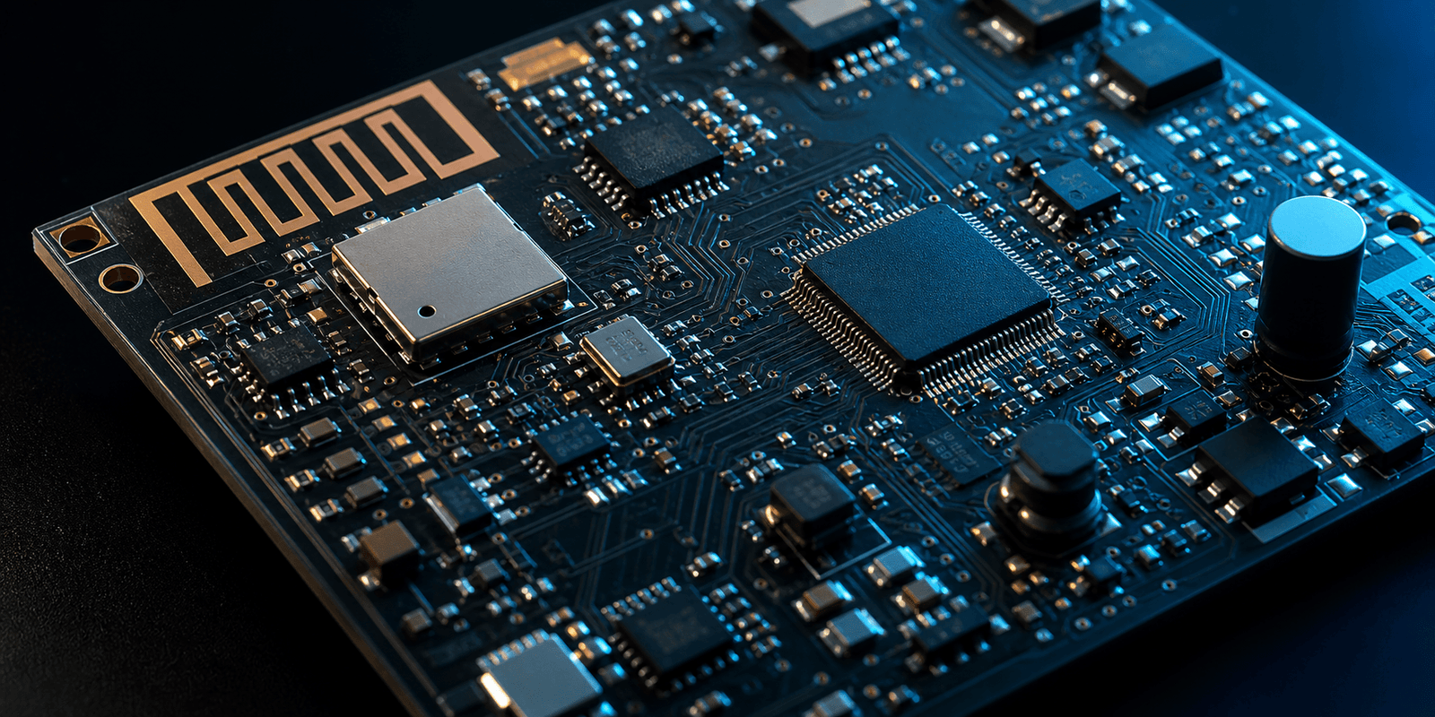
Why IoT Hardware Design Is Different From Standard Electronics Design
Standard electronics design asks one question: does the circuit perform its function reliably? IoT hardware design asks four more on top of that. Can the device communicate wirelessly at the required range and data rate? Can it run on a constrained power supply for months or years? Does it read sensor data accurately in the real world? Will it pass regulatory certification?
Each of those questions has a well-documented failure mode. Lab-measured wireless range does not survive a factory floor or outdoor installation. Bench-test battery life collapses when a peripheral misses its low-power mode. A breadboard sensor introduces PCB noise when grounding and layout are not planned. Certification testing surfaces RF emissions that force a board respin.
None of these are edge cases – they are the standard causes of IoT project delays and cost overruns. Addressing them in the architecture phase costs far less than fixing them after the first prototype.
What IoT Hardware Design Includes
A complete IoT hardware design engagement covers several interconnected areas. At Zeus Design, the electronics and IoT connectivity work flows into firmware, cloud and mobile layers – each influences the others and needs to be planned together. For a broader overview of the full development pipeline, see IoT development: hardware, firmware and cloud.
Electronics and PCB Design
The hardware foundation covers schematic capture, component selection, PCB layout, power supply design, and preparation for manufacture. For IoT devices this includes antenna placement and RF layout, sensor interface routing, battery management circuitry, and any industrial or environmental protection requirements such as conformal coating or ruggedised enclosures. Zeus Design’s circuit board design service handles multi-layer PCB layout with EMC-aware design practices built in.
IoT Connectivity and Wireless Design
Wireless protocol selection and RF layout are core to the service. This covers protocol evaluation, module or chipset selection, antenna design or selection, RF regulatory pre-compliance, and integration with the firmware stack. Zeus Design’s electronics design and IoT connectivity service includes connected-device architecture using Wi-Fi, BLE, cellular, LoRaWAN and other protocols suited to the application.
Embedded Firmware
The firmware layer handles sensor drivers, wireless stack integration, power management logic, over-the-air (OTA) update capability, and security. This work runs in parallel with the hardware – writing firmware before the PCB is finalised allows issues to be caught early. Zeus Design’s embedded software development is done alongside the hardware team, not handed off separately.
Cloud and Mobile Connectivity
Most IoT products need a backend to store and process device data, and a mobile or web app for end users or operators. Zeus Design also builds the cloud backend and mobile IoT integration layer, which means the data schemas, API contracts and security model are designed with the hardware and firmware in the same conversation rather than discovered during integration testing.
Wireless Protocol Selection
Wireless protocol selection is one of the most consequential decisions in IoT hardware design – and one of the hardest to reverse once a PCB is manufactured. The right answer depends on range, data rate, power consumption, network topology, spectrum licensing, and the cost and availability of certified modules. Get this wrong and you are looking at a respin, not a firmware update.
Wi-Fi (IEEE 802.11)
Wi-Fi is well suited to products that sit in a home or office, need to transfer moderate-to-large data volumes, and can tolerate higher power consumption. It benefits from ubiquitous infrastructure, mature security (WPA3), and a wide choice of certified modules. The downsides are relatively high current draw during transmission and limited range beyond the access point. Wi-Fi is a poor choice for battery-operated field devices that need multi-year battery life.
Bluetooth Low Energy (BLE)
BLE is the dominant protocol for short-range, battery-operated IoT devices. It is well suited to wearables, asset tracking tags, medical monitors, industrial sensors in local clusters, and any product that pairs with a smartphone. BLE 5.x extended range modes have pushed reliable range beyond 100 metres in open environments. Current draw during advertising and connection events is low enough to support coin-cell batteries for one to three years in many applications. The Bluetooth SIG specifications cover the full BLE 5.x feature set and power profile data.
LoRaWAN and LPWAN
Long-Range Wide Area Network (LoRaWAN) is designed for low-data-rate, long-range, ultra-low-power applications – remote sensors, agricultural monitoring, smart metering and similar use cases. Range in suburban deployments is typically 2-5 km; rural and semi-rural sites regularly achieve 10-15 km. Data payloads are small (tens of bytes per message) and duty cycle restrictions apply. The LoRa Alliance maintains the LoRaWAN specification and regional parameters for Australia, which uses the AU915 band plan.
Cellular (LTE-M, NB-IoT, 5G RedCap)
Cellular is the right choice when devices must operate anywhere with mobile coverage, without relying on local Wi-Fi or private gateway infrastructure. LTE-M and NB-IoT are the primary LPWAN cellular variants – both are supported on Australian networks. LTE-M supports voice, mobility and higher data rates; NB-IoT is better for static, low-data-rate applications. 5G RedCap (Reduced Capability) is emerging as a mid-tier option for devices needing more bandwidth than NB-IoT but lower complexity and cost than full 5G. Cellular modules add ongoing SIM and data plan costs that need to be factored into product economics from the start.
Zigbee and Thread
Zigbee and Thread are mesh networking protocols suited to home automation, building management and dense local sensor networks. Both operate in the 2.4 GHz ISM band and support self-healing mesh topologies. Thread is the basis of the Matter standard now supported by Apple, Google and Amazon. For products targeting the consumer smart home market, Matter/Thread support is increasingly expected.
Protocol Selection Criteria
- Range: How far does the device need to communicate, and in what environment?
- Data rate: What volume of data, and how often?
- Power budget: Is the device battery-powered? What is the target battery life?
- Network infrastructure: Does a gateway need to be deployed, or can existing infrastructure be used?
- Topology: Point-to-point, star, or mesh?
- Regulatory bands: What spectrum is available in the target market?
- Module availability and certification: Are pre-certified modules available to reduce RF regulatory risk?
- Security: What encryption, authentication and OTA update requirements apply?
Sensor Integration in IoT Hardware Design
Sensors are the interface between the physical world and your firmware. Get the integration right and you have accurate, stable, low-noise data from day one. Get it wrong and you are chasing calibration drift, noise floors and incorrect readings in devices that are already deployed and difficult to reach.
Sensor Interface Types
Most IoT sensors communicate via one of four standard interfaces:
- I2C (Inter-Integrated Circuit): A two-wire synchronous serial protocol. Supports multiple devices on the same bus via addressing. Low pin count, short-range, moderate data rates. Common for temperature, humidity, IMU, pressure and gas sensors.
- SPI (Serial Peripheral Interface): Four-wire synchronous protocol. Higher data rates than I2C, full-duplex, but requires more pins. Preferred for high-speed sensors such as ADCs, display drivers and flash memory.
- UART (Universal Asynchronous Receiver/Transmitter): Asynchronous serial communication. Common for GPS modules, barcode scanners and some wireless modules.
- Analogue: Some sensors output a voltage or current proportional to the measured quantity. These require an ADC on the MCU or a discrete ADC, and careful PCB layout to avoid noise pickup.
Signal Conditioning
Analogue sensor signals often require conditioning before they reach an ADC. Signal conditioning covers amplification (for low-level signals from thermocouples, load cells or strain gauges), filtering (to remove high-frequency noise before the ADC sampling stage), and impedance matching. The PCB layout decisions that affect signal conditioning include separation from switching power supplies, guard rings, differential routing and proper decoupling capacitor placement close to the sensor supply pins.
Sensor Placement and PCB Layout Considerations
Temperature sensors must not be placed near heat-generating components such as voltage regulators or high-current power stages. Environmental sensors that measure humidity or gas concentrations need physical access to the ambient environment, which influences enclosure design. IMU sensors are sensitive to vibration transmission paths through the PCB and mounting. These placement decisions connect the schematic and PCB layout work directly to the mechanical design of the product.
Calibration and Drift
Many sensors ship with factory calibration but still require in-system calibration against known references – particularly for precision temperature measurement, gas sensing and any application with tight accuracy requirements. Calibration procedures and tolerances need to be part of the product specification before hardware design finalises, because they affect both the sensor selection and the production test requirements.
Power Management in IoT Hardware Design
Power management is where IoT hardware projects most often fall short – and where the damage is hardest to undo. Battery life targets of one, two, or five years are achievable. But they require power management to be designed in from the start. Retrofitting it after the PCB is finalised rarely works.
Power Budget Analysis
A power budget accounts for the current draw of every component in every operating mode – active, idle, sleep, transmit, receive – multiplied by the fraction of time spent in each mode. The total average current, combined with the battery capacity in milliampere-hours, gives the theoretical battery life. In practice, the budget must include a margin for temperature effects on battery capacity, self-discharge, and the real-world duty cycle of the application.
Sleep Modes and Wake Cycles
Microcontrollers provide multiple sleep modes ranging from light sleep (peripherals running, fast wake) to deep sleep (only a real-time clock running, slow wake). The choice of sleep mode affects both current draw and how quickly the device can respond to events. For sensor-sampling applications, the typical pattern is: wake from sleep, power up sensor, wait for sensor stabilisation time, read sensor, transmit data if threshold exceeded, return to deep sleep. The stabilisation time for sensors is often overlooked – some temperature sensors take 1-2 seconds to stabilise after power-up, which adds significantly to the active period per cycle.
Power Supply Architecture
Battery-powered IoT devices typically use a lithium primary cell (non-rechargeable) or a lithium-ion/LiPo rechargeable cell, often combined with energy harvesting (solar, vibration) in longer-life installations. The power supply architecture must provide stable voltage to sensitive components across the full battery discharge curve – a 3.7 V LiPo can discharge to around 3.0 V before the device shuts down. Low-dropout regulators (LDOs) and switched-mode power supplies (SMPS) each have trade-offs in terms of efficiency, noise and cost. Battery management ICs handle charging, protection and state-of-charge reporting. The Texas Instruments power management portfolio covers a wide range of ICs relevant to IoT applications.
Peripheral Power Switching
Switching off peripherals when they are not in use is one of the most effective ways to cut standby current. Sensors, wireless modules, SD cards and display drivers all draw power even when idle. Load switches on GPIO lines let the firmware cut power to entire subsystems. Making this work requires the hardware team to include the load switches in the schematic and the firmware team to manage the wake sequence – another reason the two disciplines need to be planned together.
Compliance and Certification for IoT Hardware
IoT devices that include wireless communication must pass regulatory certification before they can be legally sold or deployed. In Australia, the relevant mark is the RCM (Regulatory Compliance Mark), which covers EMC, electrical safety and radio communications requirements under the Australian Communications and Media Authority (ACMA). Products sold in Europe require CE marking under the Radio Equipment Directive (RED 2014/53/EU). US market access requires FCC Part 15 certification for unlicensed radio devices.
The practical implication for hardware design is that RF layout, shielding, filtering, and PCB stack-up must be considered with compliance in mind from the start. Designing for pre-compliance reduces the likelihood of failing formal testing and requiring a board respin, which adds cost and time. Using pre-certified RF modules (rather than designing a custom RF front end) is the most common approach for reducing certification risk and cost – the module certification covers the radio portion, and the system integrator is responsible for the system-level integration and any additional emissions from the host PCB.
Zeus Design’s hardware design compliance service includes pre-compliance planning as part of the electronics design process, not as a separate phase after layout is complete. For a detailed breakdown of CE, FCC, UL and Australian standards as they apply to electronics products, see the regulatory considerations in electronics design resource on the Zeus Design website.
The Zeus Design IoT Hardware Design Process
Zeus Design approaches IoT hardware design as an integrated engagement covering the full product stack. The process follows a structured sequence while allowing iteration between layers as the design develops.
Discovery and Architecture
The first phase is establishing the product architecture – what the device needs to do, what it measures or controls, how it communicates, how it is powered, and what the target markets and certification requirements are. Wireless protocol selection, sensor identification and power budget estimates are produced at this stage. A clear architecture reduces rework in later phases.
Schematic and Component Selection
Schematic capture covers the full circuit design – MCU selection, sensor interfaces, power management topology, wireless module or chipset, connectors and any analogue signal conditioning. Component selection accounts for availability, lead times, cost at target volume, and qualification status. Zeus Design uses Altium Designer for schematic and PCB work, consistent with the Altium design ecosystem widely used in professional electronics development.
PCB Layout and Review
PCB layout translates the schematic into a manufacturable board. For IoT designs this includes RF layout (antenna placement, keepouts, impedance-controlled traces for RF lines), power plane design, decoupling strategy, sensor placement relative to noise sources and the physical environment, and DFM (design for manufacture) review to ensure the board can be assembled and tested reliably. Zeus Design’s PCB layout service incorporates EMC-aware practices throughout.
Firmware Development
Firmware development runs alongside the hardware, starting with sensor driver development and wireless stack integration on development boards before the custom PCB is available. This parallel approach means firmware is well advanced by the time prototype boards arrive, shortening the bring-up and validation cycle significantly.
Prototyping and Validation
Prototype PCBs are assembled and brought up systematically – power rails first, MCU second, then peripherals in sequence. Sensor accuracy, wireless range and battery life are measured against the design targets. Where results differ from the model, the power budget and field conditions are re-analysed. Zeus Design’s rapid prototyping service supports fast-turn prototype builds for early validation.
DFM, Compliance and Production Handover
Once the design is validated, it goes through a DFM review for production readiness, pre-compliance RF testing, and preparation of manufacturing documentation – assembly drawings, BOM, Gerbers, test specifications. The manufacturing package is then ready for a contract manufacturer (CM) to produce at volume.
How IoT Hardware Design Connects to Related Services
IoT hardware design does not exist in isolation. The hardware decisions shape the firmware, the firmware shapes the cloud architecture, and the cloud architecture shapes what the mobile or web app can do. Treating these as separate procurement items – hardware from one supplier, firmware from another, cloud from a third – is a reliable route to integration problems, cost overruns and delayed launches.
Zeus Design provides the full connected product stack:
- Electronics and PCB design – from schematic to production-ready layout
- Embedded firmware – sensor drivers, RTOS integration, wireless stack, OTA updates, security
- Cloud backend – device ingestion APIs, data storage, processing pipelines, device management
- Mobile app – iOS and Android apps for device control, monitoring and user interaction
- Compliance planning – pre-compliance RF review, RCM/CE/FCC preparation
Having a single team that understands the full stack means the data schema is designed once and used consistently from the sensor to the cloud to the app, rather than being negotiated across three supplier contracts.
FAQs
What is IoT hardware design and what does it involve?
IoT hardware design is the process of designing the electronics, PCB, power system and wireless connectivity for a connected device. It covers component selection, schematic capture, PCB layout, sensor integration, power management, RF design and compliance planning. The hardware design feeds directly into the firmware, cloud backend and mobile app layers of the product.
How do I choose the right wireless protocol for my IoT device?
The right protocol depends on range, data rate, power budget and deployment environment. BLE suits short-range, battery-powered devices; Wi-Fi suits higher-data-rate home and office applications; LoRaWAN suits long-range, low-data-rate field sensors; cellular (LTE-M, NB-IoT) suits devices that need mobile network coverage without local gateway infrastructure. Most IoT products have a single best-fit protocol, but some require multi-radio designs.
Why is power management so important in IoT hardware design?
Battery life is a core product specification for most IoT devices, and it is determined almost entirely by the hardware and firmware power management design. A poorly designed power architecture can reduce battery life from years to weeks. Power management must be analysed from the first architecture phase – it cannot be fixed reliably after the PCB is finalised without a redesign.
What compliance certification does an IoT device need in Australia?
Products sold in Australia that include radio communications must carry the RCM (Regulatory Compliance Mark), which covers EMC, electrical safety and radio compliance under the ACMA framework. Devices sold in Europe also need CE marking under the Radio Equipment Directive, and US-market devices need FCC Part 15 certification. Designing for pre-compliance from the start reduces the risk of failing formal testing and needing an expensive board respin. See Zeus Design’s compliance planning service for more detail.
How do I integrate sensors accurately into an IoT device?
Accurate sensor integration requires matching the sensor interface (I2C, SPI, UART or analogue) to the MCU, careful PCB layout to minimise noise on sensor signals, correct signal conditioning for analogue sensors, and thermal and physical placement that reflects what the sensor is measuring. Calibration procedures and drift tolerances should be specified before the hardware design is finalised, as they affect both component selection and production test requirements.
Can Zeus Design handle the full IoT product stack – hardware, firmware, cloud and app?
Yes. Zeus Design delivers electronics design, embedded firmware, IoT connectivity, cloud backend and mobile app development from a single Australian team. Working with one team across the full stack eliminates the integration problems that arise when hardware, firmware and software are developed by separate suppliers with different data models and assumptions.
What is the typical timeline for an IoT hardware design project?
A typical IoT hardware project from architecture to validated prototype takes four to eight months depending on complexity. A simple single-radio sensor device with an established MCU platform can be faster; a multi-protocol device with custom analogue sensing, ruggedised enclosure and compliance certification will take longer. Running firmware development in parallel with hardware design shortens the overall schedule compared to sequential approaches.
Conclusion
IoT hardware design is a layered problem. Wireless protocol selection, sensor integration, power management and compliance all interact – a decision in one area constrains the options in others. The teams that get to production on time and on budget are the ones that resolve those interactions in the architecture phase, not after the first prototype fails.
The most effective way to reduce IoT product risk is to work with a team that understands the full stack – hardware, firmware, cloud and mobile – and manages the interactions between layers from day one. Zeus Design has delivered connected products across industrial, commercial and consumer applications. If you are planning an IoT product or need a second opinion on a design in progress, get in touch with Zeus Design to discuss your project.

0 Comments