
For product managers, startup founders and engineering leads evaluating PCB designers, the hardest part is not finding candidates – it is knowing what separates a designer who produces a clean prototype from one who can take a board through to production at yield. This guide covers the practical signals to look for: EDA tool proficiency, design for manufacture (DFM) knowledge, board complexity experience and production handover capability.
TL;DR
- PCB designers range from layout-only contractors to engineers with full DFM, signal integrity and firmware integration capability – know what your project needs before you look.
- Tool proficiency matters, but the tool used (Altium, KiCad, OrCAD) is less important than whether the designer can produce clean, documented, production-ready output from it.
- DFM knowledge is the single biggest differentiator between a designer who produces a working prototype and one who can take a board through to production at yield.
- Production experience – board layers, high-speed signals, controlled impedance, component sourcing constraints – separates designers who have shipped hardware from those who have only prototyped.
- Integrated design houses that combine PCB layout with schematic design, firmware and DFM reduce handover friction and design-iteration cycles.
- Zeus Design provides PCB design and layout as part of an integrated electronics design service, based in Australia.
Why the Choice of PCB Designer Shapes Your Whole Project
Most product teams focus their due diligence on the electronics engineer who will own schematic design or the firmware team who will write device code. PCB layout is often treated as a downstream task – someone takes the schematic and does the layout. That framing underestimates how much the PCB designer’s decisions affect everything from board yield and cost to EMC compliance and production lead time.
A PCB designer makes hundreds of decisions that are not visible in the schematic: component placement, trace routing strategy, layer stack-up, via sizing, copper pour management, thermal relief, silkscreen clarity and test point positioning. Each decision affects how reliably the board assembles, how it performs under real operating conditions and how much it costs to manufacture at scale.
For a startup shipping a first hardware product, the consequences of poor PCB design decisions often surface late – during bring-up testing, pre-compliance EMC sweeps or the first production run. At that stage, a board redesign can cost months and significant budget. Evaluating PCB designers carefully at the start is far cheaper than correcting their work at the end.
The challenge is that PCB design capability is not easy to assess from a CV or a portfolio of renders. This guide gives you a practical framework for asking the right questions and interpreting the answers. If you want background on the PCB design process itself first, see the PCB design process: layers, costs and what to expect.
What PCB Designers Actually Do – and What They Do Not
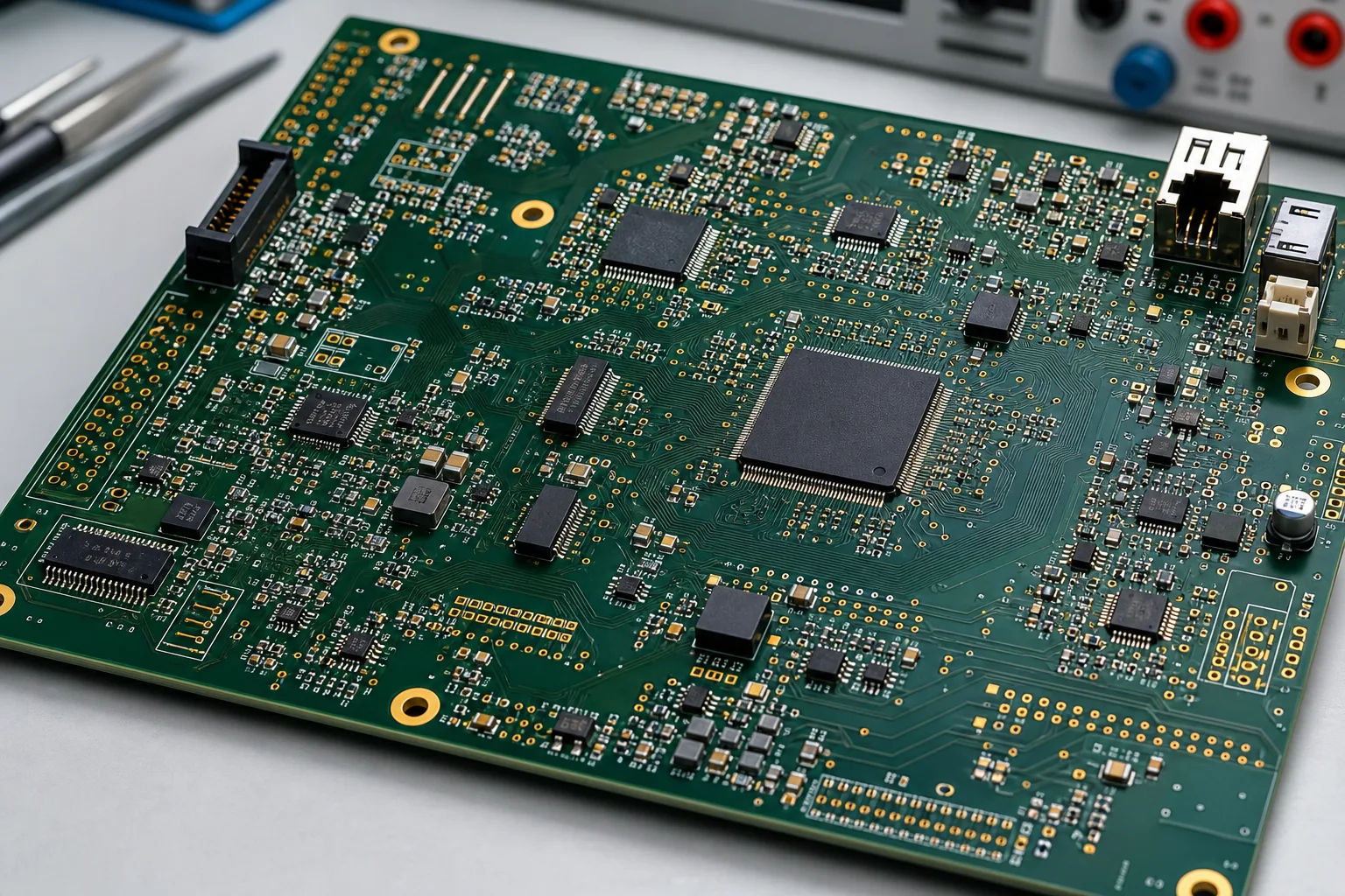
A PCB designer is an engineer or technical specialist who translates a circuit schematic into a manufacturable board layout – defining layer stack-up, placing components, routing signal traces, and generating the fabrication outputs a contract manufacturer needs to build the board. The role sits between circuit design and physical manufacturing, and the quality of work done at this stage directly determines whether a board assembles reliably and performs as designed.
Before evaluating candidates or firms, get precise about what you are buying. PCB design covers a defined scope, and practitioners vary considerably in how much of that scope they actually own.
A PCB designer’s core work includes:
- Importing or drawing the schematic netlist into an EDA tool
- Defining the board outline, layer stack-up and design rules
- Placing components in a logical, thermally and mechanically sensible arrangement
- Routing signal traces, power planes and ground pours to meet electrical and EMC requirements
- Running design rule checks (DRC) and electrical rule checks (ERC)
- Generating manufacturing outputs: Gerber files, drill files, BOM, pick-and-place files, IPC-D-356 netlist
- Preparing assembly drawings and silkscreen for contract manufacturer handover
What a layout-only PCB designer typically does not own:
- Schematic capture and circuit design decisions
- Component selection and BOM optimisation
- Firmware integration and hardware-software co-design
- DFM review and manufacturing liaison (unless specifically scoped)
- Compliance pre-planning for EMC, safety or wireless certifications
This distinction matters when you are scoping work. If you have a strong schematic designer and need layout execution only, a specialist PCB layout contractor can be a reasonable fit. If you need the PCB designer to own DFM, communicate with your contract manufacturer and flag component availability issues, you need someone with broader production experience – or a firm where those roles overlap by design.
Tool Proficiency: What EDA Software Choice Signals
The three dominant professional EDA tools for PCB layout are Altium Designer, Cadence OrCAD and KiCad. Siemens PADS and Zuken CR-8000 appear in enterprise and defence work. Each tool has genuine strengths and the choice alone does not determine designer quality. What matters more is depth of use.
A designer who has used Altium Designer for ten years, maintains a well-structured component library, uses differential pair routing tools correctly and knows how to export clean, CM-ready Gerber outputs is more valuable than someone who has touched five tools at surface level. When evaluating tool proficiency, look for:
- Library management discipline – does the designer maintain their own component libraries or rely entirely on ad-hoc imports? Library quality directly affects footprint accuracy and BOM integrity.
- Design rule configuration – can they set up and justify their DRC constraints from scratch, or do they rely on default rules? Default Altium rules are not production-appropriate for most projects.
- Output generation experience – have they handed Gerbers directly to a contract manufacturer before? Do they know how to configure drill file formats, layer naming conventions and impedance stack-up documentation?
- Revision control practice – how do they manage design iterations? Serious PCB designers version-control their design files, not just the outputs.
For most Australian product teams, Altium Designer is the dominant tool in professional design houses. If you are engaging a local firm, Altium proficiency is a reasonable baseline expectation. KiCad has matured significantly and is a legitimate professional tool, particularly for open-source-adjacent or cost-sensitive projects. Designers who work exclusively in older legacy tools without a clear reason for it may be working in an outdated workflow.
DFM Knowledge: The Production-Readiness Test
Design for Manufacture (DFM) is the discipline of designing a PCB so that it can be reliably assembled, tested and produced at the volumes you need. It is the single most important dimension to probe when evaluating PCB designers for any project that will move beyond one-off prototypes.
DFM in PCB design covers a wide range of considerations. The IPC (Association Connecting Electronics Industries) publishes the industry-standard guidelines – IPC-2221 for generic PCB design, IPC-7351 for surface mount land pattern design and IPC-A-600 for acceptability standards. A designer with genuine DFM knowledge will reference these standards without prompting and will have opinions about where their design choices sit relative to them.
Key DFM areas to probe when assessing a designer:
Solder Mask and Paste Aperture Sizing
Fine-pitch components (0.4 mm QFN, 0201 passives, BGA packages) require precise solder paste aperture sizing to avoid bridging or insufficient solder. A PCB designer with assembly experience will have calibrated paste aperture recommendations from real production feedback, not just from IPC tables.
Component Placement for Assembly
Pick-and-place machines require adequate clearance around components and consistent component orientation. A designer who has worked with a contract manufacturer directly will place components with panel rotation, fiducial placement and nozzle access in mind. One who has only worked on one-offs may create placement patterns that increase assembly rework risk.
Thermal Management
Power components, voltage regulators and high-current traces need thermal relief that matches the board’s operating environment and assembly process. Poorly designed thermal pads cause cold solder joints or overheating in production. This is an area where asking to see a specific example from a past project is informative.
Controlled Impedance and Stack-Up
High-speed digital signals (USB, HDMI, Ethernet, DDR memory) require controlled impedance traces matched to the board’s layer stack-up. Getting this wrong causes signal integrity failures that may not appear until testing at full speed or over temperature. A designer with real high-speed experience will talk about their stack-up selection process and their relationship with the PCB fabricator’s controlled impedance specification service.
Test Point Access
Production boards need test points accessible to bed-of-nails or flying-probe testers. A DFM-aware designer places test points deliberately, with probe spacing and landing pad size matched to the tester being used. Boards with no test points – or test points placed only as an afterthought – create production test cost and coverage problems.
A useful interview question is: “Walk me through how you approach DFM on a new project.” A strong answer will reference specific manufacturing constraints, CM communication and standards. A weak answer will describe running DRC and checking that the design looks clean in the viewer.
Production Experience and Board Complexity
Portfolio depth tells you more than credentials. When evaluating PCB designers, ask specifically about boards they have taken through to production – not just prototyping. For more on what this role covers day-to-day, see what a PCB designer does: skills and services explained.
Ask about these complexity dimensions specifically:
- Layer count – a designer who has only worked on 2-layer boards has not dealt with inner-layer signal routing, buried or blind vias, or multi-power-domain plane partitioning. Most commercial IoT or embedded products use 4-6 layers minimum.
- High-density interconnect (HDI) – products with BGA processors or dense RF modules may require microvias and HDI design rules. This is a specialist area and not all designers have it.
- Mixed-signal design – boards that combine analog sensing, digital processing and power regulation require careful partitioning. Ground plane management, analog and digital domain separation and power sequencing are areas where experienced designers add real value.
- RF and wireless – antenna placement, RF trace matching, keepout zones and regulatory compliance pre-planning for Wi-Fi, Bluetooth or cellular modules require specific RF layout knowledge.
- Board-level compliance experience – has the designer worked on boards that went through EMC pre-compliance testing? Can they describe how layout changes were made in response to test results?
For Australian product teams, it is also worth asking about experience with local contract manufacturers and Australian regulatory requirements. A designer who has worked with Australian CMs understands local lead times, PCB fabrication capabilities and assembly line constraints that offshore-only designers may not have encountered.
Integrated Teams vs Freelancers vs Design Houses
The engagement model you choose shapes the integration risk as much as the designer’s individual skill. Three options are available, each with a different risk and capability profile.
| Model | Best fit | Key risk | Typical scope |
|---|---|---|---|
| Freelance PCB designer | Simple boards with a complete schematic ready | No one owns the schematic-layout interface | Layout execution only |
| Specialist PCB design firm | Complex layout work with your own engineering team | Boundary risk with firmware and DFM | Layout plus CM liaison |
| Full-service design house | Products spanning PCB, firmware and production | Higher engagement cost | End-to-end: schematic, layout, DFM, firmware |
Freelance PCB Designers
Freelancers on specialist engineering platforms can offer fast turnaround and competitive rates for defined, well-scoped layout work. The risk is that a freelancer is handling layout in isolation from schematic design, component selection and firmware – which means design decisions at each layer can conflict without anyone owning the interface. For simple, low-layer-count boards where you already have a clean, complete schematic, this can work. For complex products or first-time hardware teams, the coordination overhead and integration risk is significant.
Specialist PCB Design Firms
PCB-focused design firms offer deeper layout capability and often have established CM relationships. The limitation is that they are still typically delivering a layout artefact rather than an integrated product design. If your project has firmware, wireless connectivity or complex power management, the boundary between the PCB design firm and your other engineering resources becomes a risk point.
Full-Service Electronics Design Houses
An electronics design house that combines circuit design, PCB layout, firmware development and DFM review under one roof eliminates most of the inter-discipline integration risk. The PCB layout is done by people who understand the schematic, who are talking to the firmware engineers about signal routing constraints, and who have DFM experience from taking previous products through production. The trade-off is higher engagement cost and less flexibility for teams that only need one specific service.
For hardware startups and product teams going from concept to first production run, an integrated design house model typically reduces total project cost and schedule risk even if the headline rate appears higher than a freelancer quote. Redesign cycles caused by integration failures are expensive.
How to Evaluate a PCB Designer – a Practical Checklist
Use these questions and criteria when assessing any PCB designer or design team:
- Tool depth: What EDA tool do you use, and can you walk me through how you set up DRC rules for a new project?
- DFM track record: Can you describe a specific DFM change you made in response to feedback from a contract manufacturer or assembly technician?
- Production history: How many boards have you taken from layout through to production? What were the highest layer counts and most complex component packages you have worked with?
- Output package: What does your standard CM handover package include? (Look for: Gerbers, drill files, IPC netlist, BOM, assembly drawings, impedance stack-up notes.)
- Interface ownership: If you are doing layout only, how do you handle design questions that require schematic changes? Who manages that interface?
- Compliance awareness: Have you designed boards that needed EMC pre-compliance testing? What layout changes resulted from that process?
- Component library management: How do you manage your component library? Can I see an example library entry?
- Revision workflow: How do you version-control design files and communicate design change requests?
A designer who answers these fluently, with specific examples, is demonstrating genuine production experience. Vague answers or deflection to “we follow best practices” without specifics is a warning sign.
How Zeus Design Approaches PCB Layout and Board Design
Zeus Design’s circuit board design service treats PCB layout as an integrated engineering discipline, not a downstream drafting task. Layout engineers work alongside the circuit design team from schematic capture through to production handover, so DFM constraints, signal integrity requirements and component sourcing decisions are factored in during design – not retrofitted later.
Every engagement covers multilayer stack-up selection, controlled impedance routing for high-speed signals, mixed-signal partitioning, RF keepout and antenna placement for wireless products, and a full CM handover package – Gerbers, assembly drawings and IPC netlists. DFM review is part of the layout process, not a separate add-on.
For projects that span PCB design, firmware and IoT connectivity, Zeus Design’s electronics design service integrates all three disciplines under a single engagement, which reduces handover friction and the design iterations that typically occur at discipline boundaries. For teams at the circuit board design services stage and looking for a locally based Australian partner, Zeus Design’s team has direct experience with Australian contract manufacturers and regulatory requirements.
For teams that need rapid board validation before committing to a full production design, the rapid prototyping service provides quick-turn functional PCB builds with DFM considerations built in from the first iteration.
FAQs
What qualifications should PCB designers have?
The most relevant qualification is the IPC CID (Certified Interconnect Designer) or CID+ credential, which validates proficiency in PCB design standards and DFM practices. That said, production experience and a portfolio of shipped hardware is more meaningful than certification alone. Look for designers who can reference specific IPC standards by number and describe how they applied them. Practical experience with a contract manufacturer is a stronger signal than academic qualifications for most commercial product development work.
What EDA tools do professional PCB designers use in Australia?
Altium Designer is the dominant professional tool in Australian electronics design houses and is widely supported by local contract manufacturers who accept Altium-native files in addition to Gerbers. KiCad is a capable open-source alternative used for some commercial projects. Cadence Allegro and Siemens PADS appear in larger enterprise and defence contexts. The tool matters less than the designer’s depth of use – ask about library management, DRC configuration and CM output generation, not just which software they open.
How do I know if a PCB designer has real DFM experience?
Ask them to describe a specific DFM change they made in response to assembly feedback or a CM review. A designer with genuine DFM experience will have a concrete example – solder paste aperture adjustment, thermal relief modification, test point repositioning – and will be able to explain why the change was needed. Designers who can only describe DFM in terms of running a DRC check or consulting a generic checklist have not done it under real production conditions. See Zeus Design’s electronics design service for an example of DFM-integrated board design.
Should I hire a freelance PCB designer or a design house?
For a well-defined, low-complexity layout task where you have a complete, clean schematic and no firmware integration requirements, a freelancer can be a cost-effective option. For products with high-speed digital signals, RF connectivity, complex power management or a path to volume production, an integrated design house that owns schematic, layout and DFM together reduces redesign risk significantly. The hidden cost of integration failures between separate contractors typically exceeds the rate difference on any non-trivial hardware project.
What should a PCB design deliverable include?
A production-ready PCB design deliverable should include: Gerber files (one per layer, correctly named), NC drill files, IPC-D-356 netlist, centroid or pick-and-place file, BOM with manufacturer part numbers and approved alternates, assembly drawings showing component orientation and polarity, controlled impedance stack-up documentation if applicable, and a design rule check report. Designers who deliver only Gerbers without the supporting documentation create downstream problems for your contract manufacturer and quality team.
What board complexity should I expect a professional PCB designer to handle?
A professional PCB designer should be comfortable with 4-6 layer boards, SMD components down to 0402 and QFN packages, differential pair routing, and power and ground plane management. Experienced designers will also handle HDI (microvias, blind and buried vias), BGA routing, controlled impedance for high-speed signals, and RF layout constraints. Ask specifically about the most complex board the designer has taken to production, not just the most complex they have laid out. Production experience reveals competency that prototype-only work does not.
How do PCB designers handle changes after layout is complete?
Professional designers use version-controlled design files and a formal Engineering Change Order (ECO) process for post-layout modifications. Ad-hoc changes without version control are a real risk: a schematic change not propagated correctly through to layout is a common source of bring-up failures. Ask how the designer manages changes and how they communicate the layout impact of schematic revisions back to the circuit design team. How they answer tells you a lot about process maturity.
Published May 2026. Reflects current EDA tool landscape, IPC standards and Australian electronics design market conditions.
Conclusion
Choosing the right PCB designers for your hardware project comes down to three things: tool proficiency that produces clean, documented, CM-ready output; genuine DFM knowledge developed through real production experience; and the right engagement model for your project’s integration complexity. For teams building products with high-speed signals, wireless connectivity or a defined path to production volume, an integrated design approach – where PCB layout, schematic design and DFM review are owned by the same team – is consistently lower risk than coordinating separate specialist contractors.
Zeus Design’s engineering team works with Australian product companies from first schematic through to production-ready board design. If you need to scope PCB design, rapid prototyping or a full electronics design engagement, reach out to discuss your project requirements.





0 Comments