
Test jig development is one of the most underinvested steps in electronics product development – and for engineering managers, founders and product teams moving a PCB design into volume production, getting the test strategy right early directly affects yield, quality and unit cost. This guide covers the full test jig development process: from test specification through fixture design, design for testability, automation and production-line integration. It also explains how Zeus Design’s test jig development service fits into a broader electronics design and manufacture engagement.
TL;DR
- A test jig is a custom mechanical and electrical fixture that holds a PCB and connects it to test equipment for repeatable, automated quality checks on the production line.
- The main types are in-circuit test (ICT) fixtures, functional test jigs, programming fixtures and flying-probe rigs – each suited to different volumes, board complexity and test coverage requirements.
- Test jig development starts during PCB design, not after it – design for testability (DFT) decisions made early prevent expensive redesigns and poor test coverage later.
- A well-designed test jig reduces per-unit test time, catches defects at the earliest point in the production flow (where they are cheapest to fix), and produces structured pass/fail data for production monitoring.
- Zeus Design develops test jigs as part of its electronics design service, aligned with PCB layout, firmware and DFM work so the fixture is ready when the board goes into production.
Why Test Jigs Matter in Electronics Production
When a PCB design moves from prototype to production, workbench testing – probing with a multimeter, watching a debug console, manually cycling the device – no longer scales. At even modest volumes of a few hundred units per month, manual inspection becomes a bottleneck, defects slip through, and rework costs accumulate. A production test jig makes testing repeatable, fast and operator-independent.
The economics are straightforward. The electronics industry applies the “Rule of Ten” to defect detection cost: a fault caught at PCB test costs roughly ten times less to fix than the same fault caught at system integration, and roughly a hundred times less than a fault that reaches a customer. Test infrastructure is not overhead – it is risk management built into the production process.
For product teams planning a move to production, the question is not whether to test, but when to invest in a dedicated fixture and what coverage it needs. That depends on volume, board complexity, regulatory requirements and the cost of a field return.
What Test Jig Development Covers
Test jig development spans the mechanical, electrical and software elements needed to test a specific PCB assembly reliably at production rate. Key deliverables include:
- Test specification – a document defining what the fixture must verify: which electrical nodes, what functional behaviours, what pass/fail criteria, and what test coverage percentage is required.
- Fixture design – mechanical CAD for the housing, alignment guides, actuation mechanism (pneumatic, manual clamp or lever press) and pogo-pin layout that contacts the board’s test points.
- Test electronics – a controller board or interface to external test equipment (multimeter, oscilloscope, power supply, signal generator or a dedicated ICT system) that exercises the board under test.
- Test software – firmware or PC-side scripts that sequence the test, apply stimuli, measure responses and produce a structured pass/fail result with traceability data.
- Validation and handover – running the jig on known-good and known-bad boards to verify it catches target defects, then documenting it for production operators.
Types of Test Jig
The four main fixture types each serve a different purpose in the test strategy:
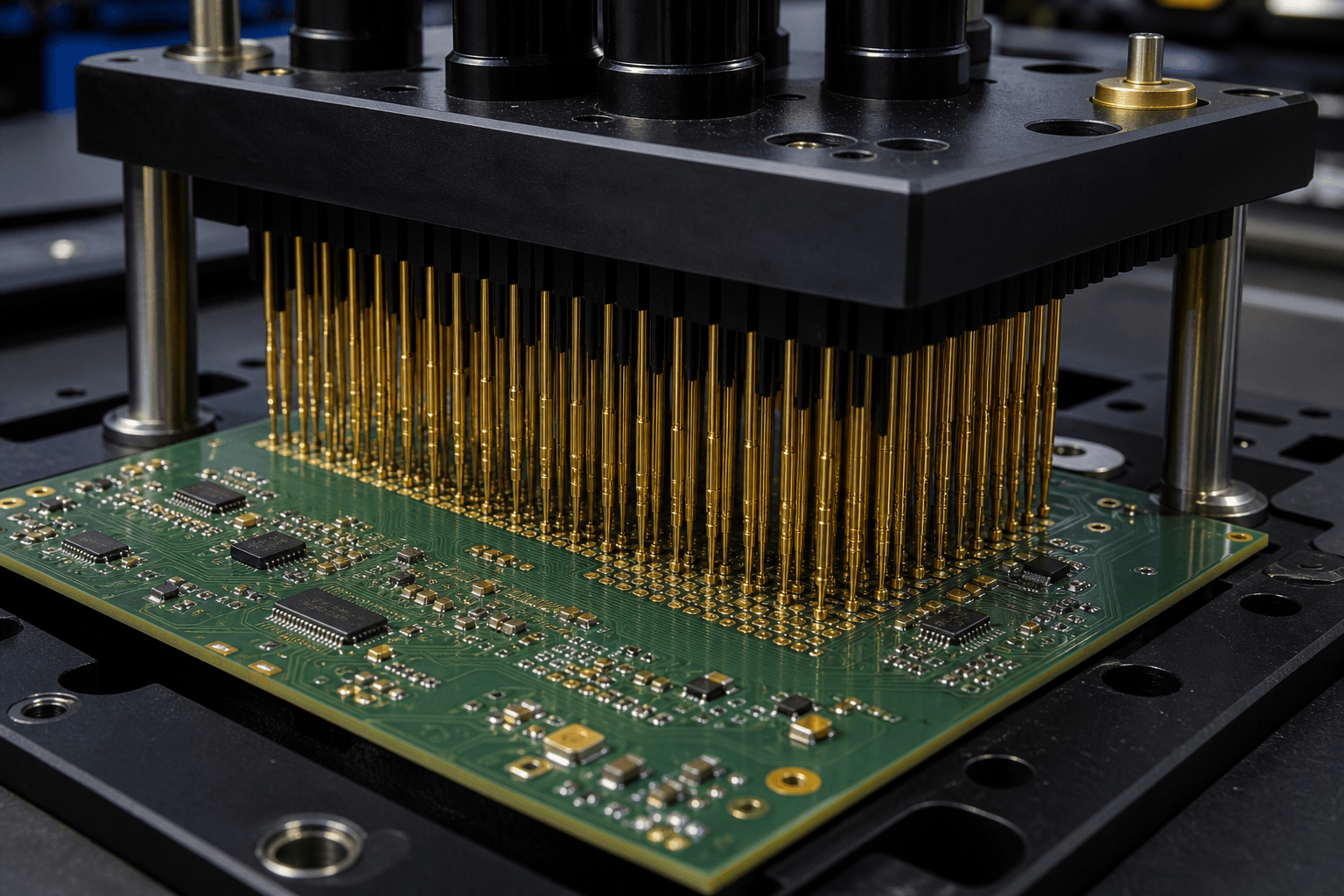
In-Circuit Test (ICT) fixtures use a bed-of-nails arrangement – an array of spring-loaded pogo pins that simultaneously contact hundreds or thousands of test points on the assembled board. The ICT system measures individual component values, checks for short circuits, open joints and missing components, and typically completes a full board check in under a minute. ICT fixtures carry significant upfront cost (fixture fabrication plus test program development), but per-unit test cost at volume is very low. According to SPEA’s in-circuit testing guide, ICT is well suited to detecting soldering defects, component placement errors and open circuits – the majority of assembly faults.
Functional test (FCT) jigs test the assembled board the way the end product will be used – applying power, exercising firmware, driving inputs and measuring outputs. Connection is via pogo pins or direct connectors, with the jig typically running a test script from a PC. Functional testing confirms correct behaviour rather than just correct assembly, and is most valuable when the BOM is straightforward but firmware behaviour is complex.
Programming fixtures are a specialised subset that focus on loading firmware and calibration data onto microcontrollers or flash memory during production. They use a gang programmer or single-unit programmer accessed via pogo pins on JTAG, SWD or UART pads. Many production test jigs combine programming and functional test in a single fixture to reduce handling time.
Flying-probe rigs use a small number of motorised probes (typically four to eight) that move across the board under software control, testing points sequentially. Flying probe requires no custom fixture and is well suited to prototype or low-volume production where the design may still change and a fixture investment cannot yet be justified. The trade-off is test time – sequential probing is slower than simultaneous contact.
When Your Project Needs a Custom Test Jig
Not every project needs a bespoke fixture from day one. The right time to invest depends on several factors:
- Production volume – once you are building more than a few hundred boards per month, the time saved by a fixture versus manual testing or flying probe pays back the upfront development cost quickly. For most consumer or industrial products, the crossover point falls somewhere between 200 and 500 units per production run.
- Board complexity – a dense multilayer board with many signal nets, power rails and peripheral interfaces benefits from high test coverage that only a bed-of-nails ICT fixture or a structured functional test jig can provide.
- Regulatory requirements – some product categories (medical, industrial safety, automotive) require documented test coverage and traceability for every unit shipped. A custom jig with structured pass/fail logging is often the only practical way to meet these requirements.
- Firmware complexity – products where correct firmware behaviour is the primary quality criterion (IoT devices, motor controllers, sensor nodes) need functional testing that verifies behaviour, not just assembly.
- Field return risk – if a defective unit reaching a customer carries a high cost (warranty repair, recall, reputational damage, safety liability), the economics of a thorough test fixture are easy to justify even at modest volumes.
Design for Testability: Getting the PCB Right First
Test jig development and PCB design are tightly coupled. A layout designed without testing in mind produces a fixture that is difficult to build, covers fewer nets than needed, or requires probe positions that create mechanical reliability problems.
The key design for testability (DFT) practices that make test jig development straightforward are well documented in resources such as Altium’s DFT design guide:
- Test point placement – adding dedicated, solder-mask-free copper pads on every net that needs to be probed, positioned on one side of the board to allow single-side fixture access. A spacing of at least 2.5 mm between test point centres is the standard clearance for bed-of-nails probe heads.
- 100% net accessibility – aiming for at least one accessible test point on every electrical net so that the test program can verify every node. Inaccessible nets are defect escape routes.
- Alignment features – dedicated tooling holes or fiducials that the fixture uses to locate the board accurately. Without precise alignment, pogo pins miss their target pads and cause false failures or fixture damage.
- Connector and programming pad placement – positioning JTAG, SWD, UART and power connectors consistently so that a single-side fixture can access them without special adapters.
- Keepouts around test points – ensuring tall components (capacitors, connectors, heat sinks) do not obstruct the probe travel path of the fixture’s pogo pins.
When Zeus Design develops a PCB layout as part of an electronics design engagement, DFT requirements are incorporated during the layout phase – not reviewed afterwards. This matters most for design for manufacture (DFM) work, where test strategy, fixture type and expected production volume are known inputs that shape layout decisions from the start. For a broader look at how PCB layout decisions affect the entire product lifecycle, see PCB Design: Process, Layers, Costs and What to Expect.
Risks to Plan For Before You Commit to a Fixture
Several failure modes recur across test jig projects. Understanding them early prevents the most costly mistakes:
Pogo Pin Wear
Pogo pins wear over repeated contact cycles – typically rated for 100,000 to 500,000 cycles depending on pin design and spring force. In high-volume production, a pin set can reach that limit in weeks. Design the fixture for easy pin replacement, and include a self-test routine in the test program to catch degraded contact resistance before it causes false failures.
Test Coverage vs. Test Time Trade-off
More coverage means more probe points and longer test sequences, adding per-unit test time and fixture cost. The right balance comes from ranking defects by probability and impact, then building coverage around the highest-risk nets first. Chasing 100% ICT coverage on a 2,000-net board will often cost more in fixture complexity than the marginal defect risk justifies.
Board Revision Coupling
A bed-of-nails fixture is specific to a single board revision. If the PCB layout changes – even a minor component relayout that moves test points – the fixture may need rework or replacement. For products still in active development, start with flying-probe testing and transition to a dedicated fixture once the design is stable.
False Confidence from Incomplete Validation
A jig that passes known-bad boards is worse than no jig – it creates false confidence. Before production use, validate the fixture against deliberately faulted boards covering the defect types it is supposed to catch: missing components, solder bridges, wrong component values and open joints at minimum.
Software and Calibration Drift
Test programs using absolute voltage or current thresholds need calibration verification as equipment ages. Build calibration checks into the fixture startup sequence, and keep threshold documentation version-controlled alongside the PCB design files.
How Zeus Design Approaches Test Jig Development
Zeus Design builds test jigs within its broader electronics design and test systems service, timed to the product development schedule so the fixture is ready when the first production boards arrive:
- Test specification – early in the project, Zeus Design works with the product team to define what needs to be tested, what coverage is required, what the acceptable test time per unit is, and what traceability data needs to be captured (serial number, test date, firmware version, pass/fail log).
- DFT review – before the PCB layout is finalised, the test specification drives a design for testability review. Test point positions, tooling holes, connector locations and keepout zones are confirmed or added to the layout at this stage.
- Fixture mechanical design – CAD design of the fixture housing, alignment mechanism, pogo-pin layout and actuation (manual, lever or pneumatic). Materials selection for the fixture body considers durability, dimensional stability and ease of machining – anodised aluminium for the structural frame, acrylic or FR4 for probe guide plates.
- Test electronics and firmware – design and build of the fixture controller board and test software. For simple functional jigs this may be a microcontroller-based controller; for full ICT systems it interfaces to bench test equipment or a dedicated ICT platform.
- Prototype fixture build and validation – the first fixture is built and validated against pre-production boards, covering both known-good and known-bad specimens to verify test coverage and false-failure rate.
- Production handover – the validated fixture, test program, calibration procedure and operator instructions are handed over to the contract manufacturer or production team.
For products developed end-to-end with Zeus Design – from circuit design and PCB layout through firmware and production – the test jig shares design files, component libraries and firmware toolchain with the product, which reduces integration effort and makes future fixture revisions straightforward.
How Test Jig Development Connects to the Rest of Your Project
Test jig development rarely stands alone. It works best when integrated with the surrounding design and production work:
PCB and Circuit Design
Layout choices made during PCB design and layout determine what is testable and at what cost. DFT is cheapest to incorporate during the layout phase – adding test points costs nothing at that stage, while retrofitting them to a finished layout can require significant rerouting. Zeus Design’s PCB design service includes DFT review as a standard step.
Embedded Software Development
Functional test jigs rely on firmware running on the board under test to respond to stimuli in predictable ways. For boards developed with Zeus Design’s embedded software development service, a test mode or manufacturing mode can be built into the firmware to support structured functional testing without requiring the full application software stack to be operational. See Embedded Software Development: A Guide for Hardware Teams for more on how firmware architecture choices affect production and test.
Design for Manufacture
Test jig development sits within the broader design for manufacture (DFM) process. DFM decisions about component selection, board panelisation, solder paste stencil design and assembly process all shape what test strategy is practical and what coverage is achievable. Zeus Design’s design for manufacture service treats test strategy as part of the production-readiness work – not an afterthought.
Rapid Prototyping
Before a production fixture is warranted, Zeus Design’s rapid prototyping service supports hands-on functional testing using bench equipment and simple programming fixtures – building the test knowledge that feeds into the production fixture specification.
FAQs
What is test jig development and why does my product need it?
Test jig development is the process of designing and building a custom fixture that holds a PCB and connects it to test equipment to verify quality on a production line. Your product needs it once manual testing cannot keep pace with production volume, or when regulatory requirements demand documented per-unit test coverage. A well-designed jig catches defects at the earliest – and cheapest – point in the production flow.
At what production volume does a custom test fixture make sense?
For most electronics products, the investment in a custom bed-of-nails or functional test fixture pays back once you are building several hundred units per production run. Below that threshold, flying-probe testing or a simple programming and power-on functional jig often provides the best balance of coverage and cost. Zeus Design can help you model the crossover point for your specific product based on board complexity, test time targets and defect risk.
What is the difference between ICT and functional testing?
In-circuit testing (ICT) checks individual components and solder joints by probing every accessible net on the board simultaneously – it verifies that the board was assembled correctly. Functional testing exercises the board the way the finished product operates – applying power, running firmware and measuring behaviour. ICT catches assembly defects; functional testing catches design or firmware faults that survived assembly. Many production lines use both in sequence, with ICT upstream and functional test downstream.
How long does test jig development take?
A straightforward functional test jig with a simple PCB controller and manual clamp mechanism typically takes four to eight weeks from specification to validated fixture. A full bed-of-nails ICT fixture for a dense multilayer board, including fixture fabrication, test program development and validation, can take eight to fourteen weeks. Starting test jig development in parallel with the final PCB layout phase – not after the board is in production – avoids this lead time becoming a bottleneck.
Can the test jig also program firmware during production?
Yes. Combining firmware programming and functional testing in a single fixture is common practice for IoT and embedded products. The fixture loads the production firmware image via a pogo-pin JTAG or SWD interface, then immediately runs the functional test sequence. This single-step approach reduces handling, ensures firmware and test are version-matched, and simplifies the production workflow. Zeus Design’s embedded software development service supports manufacturing test mode firmware as a standard deliverable for products developed end-to-end.
What happens to the test jig when the PCB design changes?
A bed-of-nails fixture is specific to a board revision – if test point positions move, the probe guide plate needs to be remachined and the test program updated. This is why it is important to stabilise the design before committing to a hard-tooled ICT fixture. For products with active development cycles, Zeus Design typically recommends a flying-probe or simple functional jig for early production runs, transitioning to a dedicated fixture once the design is locked. The fixture design should be version-controlled and linked to the specific PCB revision it supports.
Conclusion
Test jig development works best when it starts with the electronics design – not after the boards are already shipping. Fixture type, test coverage requirements and DFT decisions all need to be aligned with the PCB layout, firmware architecture and production volume before the first boards go down the line.
Zeus Design develops test jigs alongside PCB design, embedded firmware and DFM work so the test strategy stays consistent with the rest of the product. If you are preparing a PCB for production and want to work out the right test approach for your volume and risk profile, the starting point is a conversation about where your design currently sits.
")


0 Comments