
Hardware design for connected products translates a product concept into verified, manufacturable electronics – covering system architecture, component selection, PCB layout, firmware integration, and compliance planning. If you are a founder, product team member or engineering manager scoping a connected or IoT product, this guide explains what good hardware design actually involves, where decisions get costly when made late, and how a full-service partner like Zeus Design approaches the work.
TL;DR
- Hardware design for connected products spans architecture, circuit design, PCB layout, firmware integration, wireless stack selection and compliance – not just schematic capture.
- Connectivity choice (Wi-Fi, Bluetooth, cellular, LPWAN) is one of the earliest and most consequential architecture decisions, affecting cost, power budget and certification requirements.
- Component selection locks in long-term supply chain risk – availability, lifecycle status and second-source options matter as much as datasheet specs.
- PCB layout directly affects signal integrity, EMC performance and test outcomes – a good schematic can still produce a poor board if layout is treated as a separate concern.
- Compliance planning (RCM, FCC, CE) should begin during architecture, not after prototyping is complete.
- Zeus Design delivers end-to-end hardware design, from electronics and PCB through to embedded software, IoT connectivity and design for manufacture.
Why Connected Products Raise the Stakes for Hardware Design
A standalone electronic product has a defined set of design constraints. A connected product adds wireless RF, power management for battery or low-power operation, antenna design, security at the hardware layer, firmware complexity and the regulatory surface area that comes with transmitting RF energy in target markets.
Those layers interact with each other in ways that are not always obvious upfront. The wireless protocol you choose influences the power budget, which shapes the battery and charging circuit, which affects the PCB footprint, which affects thermal performance and antenna clearance. Early architecture decisions cascade through every subsequent phase. Teams that treat hardware design as a checklist of component sourcing and PCB layout tend to discover these interactions too late – after prototypes fail pre-compliance testing, or after the supply chain for a key module goes end-of-life six months before launch.
This guide covers the decisions and trade-offs that matter most, structured to match the way hardware design actually unfolds on a real project.
What Hardware Design for a Connected Product Includes
Hardware design is broader than PCB design. PCB design is a critical phase within it, but the discipline spans the full arc from system architecture to production handover. For a connected product, that arc typically includes:
- System architecture: Defining the functional blocks – processor, memory, power, connectivity, sensors, interfaces – and how they relate to each other and to the intended software stack.
- Component selection: Choosing specific devices from the architecture’s functional requirements, balanced against supply chain maturity, cost, availability and long-term lifecycle status.
- Schematic design: Capturing the circuit in a way that is correct, traceable and ready for PCB layout – including power rails, reference designs, decoupling strategy and interface pinout.
- PCB layout: Translating the schematic into a manufacturable board with signal integrity, EMC and DFM requirements built into the layout decisions, not bolted on afterwards.
- Firmware integration: Bringing up the hardware with embedded software that validates each functional block and establishes the baseline for product firmware development.
- Compliance planning: Identifying which certification marks apply to the target markets and designing to meet those requirements from the first revision, not the third.
- Design for manufacture (DFM): Reviewing the design against assembly and production constraints to reduce yield risk and keep manufacturing cost within target.
Zeus Design’s electronics design service covers this full scope. The real difference between a specialist PCB layout house and an end-to-end partner shows in how those phases connect – whether firmware enters the picture after PCB layout is frozen, or whether it shapes the architecture conversation from day one.
Architecture Decisions That Drive Everything Else
Processor and memory selection
For connected products, processor choice is almost always driven by the connectivity stack, not raw processing performance. A Wi-Fi and Bluetooth SoC – such as the Espressif ESP32 family or Nordic nRF52 series – integrates the wireless stack with the application processor, cutting BOM count and PCB footprint compared to pairing a separate MCU with a discrete radio module. The trade-off: the software team works within the SoC vendor’s SDK and radio stack, which constrains certain real-time or safety-critical designs.
Products that need cellular connectivity typically use a module-based design – a separate cellular module connected to an application MCU via UART or USB. This gives more flexibility in processor selection but adds board space, BOM lines and power complexity. The right choice depends on data throughput, battery life targets, OTA update requirements, and the firmware team’s experience with each approach.
Connectivity protocol selection
Wireless protocol selection is the decision with the longest downstream consequences. The main options for connected products in 2026 are:
- Wi-Fi (802.11 b/g/n/ax): High throughput, widely understood, assumes infrastructure (router) in the field environment. Power-hungry for battery devices unless deep-sleep duty cycling is implemented carefully. RCM and Wi-Fi Alliance certification add to the compliance workload.
- Bluetooth Low Energy (BLE): Low power, short range, well-suited to wearables, peripheral sensors and direct-to-phone products. BLE 5.x extended range modes allow longer range without major power penalty. Requires a phone or gateway as the hub for cloud connectivity.
- Cellular LTE-M / NB-IoT: Direct cellular connectivity without needing a local gateway. LTE-M supports voice and mobility; NB-IoT is optimised for low-data, deep-penetration scenarios. Carrier relationships, SIM provisioning and recurring data costs add to the product lifecycle economics.
- LoRaWAN / LPWAN: Very long range, very low power, very low data rate. Suited to sensor networks and asset tracking where small periodic payloads are all that is required. Depends on network coverage or requires deploying a private gateway.
- Thread / Matter / Zigbee: Mesh networking protocols suited to smart home and building automation. Matter (built on Thread and Wi-Fi) is consolidating the smart home ecosystem and is worth evaluating for consumer connected products.
None of these is universally correct. Start the selection exercise with the product’s operational scenario – where it deploys, what data it transmits and how often, what the power budget is, and what connectivity infrastructure exists in the field. Zeus Design’s IoT connectivity capability covers this evaluation as part of the architecture phase, not as a separate deliverable.
Power architecture
For mains-powered products, power architecture is mainly about regulation quality, efficiency and protection. For battery-powered or energy-harvested products, it becomes one of the central design challenges. Regulator topology (LDO versus switching), battery chemistry and management IC, charging architecture, and the way the MCU and radio handle low-power states all interact to determine real-world battery life – which often looks nothing like the theoretical estimate from datasheet typical current figures.
Power decisions also affect PCB layout complexity. Switching regulators need careful placement and routing to contain EMI, and that problem compounds when the product also carries a sensitive RF antenna on the same board.
Component Selection for Connected Products
Component selection is not just about finding parts that satisfy the datasheet. For a connected product heading to production, these factors matter as much as electrical performance:
Supply chain maturity and lead time
The component shortages of the early 2020s permanently changed how engineering teams think about BOM risk. In 2026, lead times for certain microcontrollers, wireless SoCs and power management ICs remain higher than pre-shortage norms. Designing around parts with predictable 8-12 week lead times and established distribution across multiple channels (Mouser, DigiKey, Arrow, local Australian distributors) is a more defensible position than optimising purely on unit cost.
For wireless modules and SoCs specifically, the vendor’s product lifecycle roadmap matters. A module certified today may face EOL within the production window of a product expected to be in the field for five to ten years.
Second-source availability
For high-volume or long-lifecycle products, identifying second-source or form-fit-function equivalents at the design stage is far cheaper than retrofitting them later. This matters most for microcontrollers, memory and power management ICs, where vendor-specific peripherals or toolchains can create hard lock-in.
Reference designs and application support
Semiconductor vendors publish reference designs and application notes for good reason: they encode hard-won knowledge about real circuit behaviour, common failure modes, and layout constraints that rarely appear in the datasheet. Following reference designs closely – particularly for RF circuitry, power stages and high-speed interfaces – cuts first-spin risk substantially. Deviating without a clear engineering rationale is one of the more reliable ways to generate expensive prototype respins. Espressif’s ESP32 hardware design guidelines are a practical example of the depth a good reference design provides.
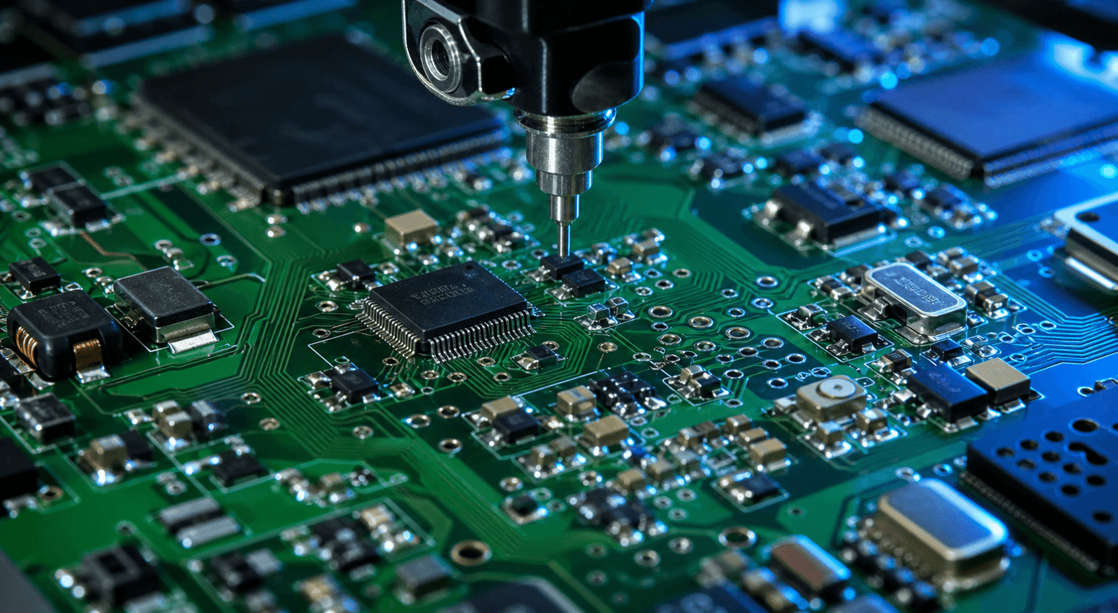
PCB Layout for Connected Products
PCB layout for a connected product is more demanding than for a purely digital product of similar complexity. RF circuitry, switching power supplies and mixed analog-digital signal paths create interactions that do not show up until the board is built and tested.
Antenna design and placement
For integrated antennas (PCB trace or chip antennas), the antenna needs adequate ground clearance and must stay clear of high-current traces, switching regulators and other RF sources. Most antenna vendors specify a keep-out zone on all copper layers. Ignoring these guidelines is a common cause of poor RF sensitivity in first prototypes – and fixing it usually requires a full board respin, not a simple patch.
For external antennas connected via U.FL or SMA, the RF trace from the SoC or module to the connector must be impedance-controlled (typically 50 ohm) and routed as a microstrip or coplanar waveguide with a consistent reference plane. That requirement directly constrains the stack-up and layer assignment decisions for the whole board.
EMC-aware layout
EMC performance is largely determined in layout, not schematic. A well-designed schematic laid out without regard for return current paths, power plane splits or clock signal coupling will fail pre-compliance testing regardless of how well the components were chosen. Key layout disciplines that affect EMC: unbroken reference planes under high-speed signals, decoupling capacitors placed close to power pins, differential pair routing for high-speed interfaces, and contained switching regulator loop area.
Zeus Design’s PCB design service treats EMC-aware layout as standard practice, not an add-on review at the end of the project.
Thermal management
Cellular modules, Wi-Fi SoCs under sustained load, and motor drive circuitry can generate enough heat to affect both reliability and regulatory compliance. Thermal vias under exposed pads, copper pours tied to internal ground planes, and component placement that supports natural convection are all layout-level decisions. In enclosure-constrained designs, thermal path planning often influences the PCB stack-up and mechanical design at the same time.
Embedded Firmware and Hardware Bringup
Hardware design does not end when Gerbers are sent to the PCB manufacturer. Bringup – powering up a new board and validating each subsystem systematically – is a phase that surfaces both hardware faults and the gaps between schematic intent and real circuit behaviour.
For connected products, bringup typically works through: power rails in sequence, crystal and clock sources, MCU boot and JTAG/SWD debug access, flash and RAM access, peripheral buses (I2C, SPI, UART), RF module initialisation and AT command response, sensor readback, and battery and charging circuit behaviour. Validate each subsystem independently before attempting full-system firmware.
Running embedded firmware development in parallel with hardware design – rather than sequencing hardware first and firmware second – closes the gap between first board assembly and functional prototype. Zeus Design’s embedded software development capability works in parallel with hardware design on integrated projects, compressing the overall development timeline.
Compliance Planning for Connected Products
Any connected product that transmits RF energy must be certified before sale in each target market. In Australia and New Zealand, the RCM mark covers both electromagnetic compatibility (EMC) and electrical safety requirements, replacing the former C-Tick and A-Tick marks. For products sold into the US, FCC Part 15 certification applies to all devices emitting RF energy, including Wi-Fi, Bluetooth, and proprietary RF protocols. European markets require CE marking under the Radio Equipment Directive (RED), EMC Directive and Low Voltage Directive depending on product type.
The core principle for managing compliance cost is straightforward: design for certification, do not redesign for it. A product that reaches pre-compliance testing with an unvalidated antenna design or a power supply whose emissions were never checked against conducted and radiated limits will almost certainly need hardware changes before certification proceeds. Those changes – board respin, re-assembly, re-test – are expensive in both time and money.
Compliance planning integrated into the architecture phase covers: selecting pre-certified modules where appropriate (which transfers some certification burden to the module vendor), identifying the applicable standards for each target market early, designing the antenna and RF front-end to the relevant test limits, and scheduling pre-compliance testing at prototype stage before committing to the production design. The ACMA equipment authorisation overview is a useful starting point for Australian teams unfamiliar with the RCM framework.
Design for Manufacture: From Prototype to Production
A prototype that works reliably on the bench is not a design that will produce consistent, low-defect boards at volume. Design for manufacture (DFM) is the set of practices that bridges that gap.
Key DFM considerations for connected products:
- Component footprints and courtyard clearances: Footprints that are accurate to IPC standards and have adequate clearance for automated placement and inspection reduce assembly defect rates significantly.
- Solder paste aperture design: For fine-pitch QFN, BGA and chip antenna packages, solder paste aperture design affects joint quality and voiding. This is something that many PCB layout tools do not optimise automatically.
- Panel and fiducial design: Boards destined for volume assembly should be designed in panels with appropriate routing, breakouts and fiducials for the pick-and-place equipment at the intended manufacturer.
- Test access: Including test points on key nets – power rails, programming interfaces, key signals – enables in-circuit test (ICT) or flying-probe test during production without redesigning the board.
- BOM standardisation: Minimising the number of unique component values (for example, using a single 100nF decoupling capacitor value where 68nF and 100nF would both work) reduces BOM line count and kitting complexity at the contract manufacturer.
DFM review is most effective when it happens during layout, not after Gerbers are complete. Zeus Design builds DFM review into the PCB design process rather than treating it as a final gate.
How Zeus Design Approaches Connected Product Hardware
Zeus Design delivers end-to-end hardware design for connected and IoT products – from initial architecture to production-ready design packages. The scope covers electronics design, PCB layout, embedded software, IoT connectivity, mobile app development and cloud backend. That means the hardware architecture is designed with the full product stack in mind from the first conversation, not reverse-engineered to fit a software team’s requirements later.
For connected product projects, that typically means:
- Architecture review that considers connectivity protocol, power budget, firmware stack and compliance requirements together – not as sequential phases.
- Schematic and PCB design with EMC-aware layout, DFM review and production readiness built in.
- Embedded firmware developed in parallel with hardware, reducing total development time.
- Compliance planning integrated from architecture, with pre-compliance test preparation before the production build commitment.
- Mobile and cloud development for the full connected product ecosystem, using the same team that designed the hardware.
This integrated approach removes the coordination overhead and the architectural gaps that appear when hardware design, firmware and software are handled by separate parties who never shared the same brief.
FAQs
What is hardware design for a connected product?
Hardware design for a connected product covers the full process of defining, designing and verifying the electronics that make up a wireless or IoT device. It includes system architecture, component selection, schematic design, PCB layout, firmware bringup, compliance planning and DFM review. It is broader than PCB design alone, though PCB design is a central phase within it.
How long does hardware design take for an IoT product?
A first functional prototype for a connected product typically takes 3-6 months from architecture freeze to assembled and validated board, depending on complexity. Production-ready design – including compliance testing, DFM review and manufacturing setup – typically adds another 2-4 months. Projects that integrate firmware development alongside hardware design can reduce overall timeline by 4-8 weeks compared to sequential approaches. See Zeus Design’s electronics design service for more on typical project timelines.
What wireless protocol should I choose for my connected product?
The right protocol depends on the deployment environment, data volume, power budget and connectivity infrastructure available in the field. Wi-Fi and BLE are appropriate for home and office environments with existing infrastructure. Cellular LTE-M or NB-IoT suits field-deployed devices that need direct cloud connectivity. LoRaWAN is suited to low-data sensor networks over long distances. Protocol selection should happen during architecture, not after the hardware is designed.
What certifications does a connected product need in Australia?
In Australia, connected products that transmit RF energy require the RCM mark, which covers both EMC and electrical safety requirements. Products sold in the US also need FCC Part 15 certification, and CE marking is required for European markets under the Radio Equipment Directive. Designing for compliance from the architecture phase – rather than retrofitting changes after pre-compliance testing – is the most cost-effective path to certification.
What is the difference between hardware design and PCB design?
PCB design is the process of translating a schematic into a physical board layout – placing components and routing connections to meet electrical, mechanical and manufacturing requirements. Hardware design is the broader process that includes system architecture, component selection, schematic design, PCB layout, and validation planning. A hardware designer makes the decisions that determine what the PCB designer is asked to implement. For connected products, both disciplines need to operate closely together because RF, power and layout decisions are intertwined.
How do I manage component supply chain risk in a connected product design?
Key practices include: selecting components with multiple distributor channels and established lifecycle status, identifying second-source equivalents at design stage for critical devices, avoiding new or niche parts where mature alternatives exist, and reviewing BOM lead times against the production start date during the design phase. For wireless modules specifically, confirming the vendor’s certification and lifecycle roadmap before committing to a module is worth doing early. Zeus Design includes supply chain considerations in component selection as part of the electronics design process.
Can Zeus Design handle both the hardware and the software for a connected product?
Yes. Zeus Design delivers end-to-end connected product development covering electronics design, PCB layout, embedded firmware, IoT connectivity, mobile app development and cloud backend. Working with a single team across hardware and software disciplines avoids the architecture gaps that appear when these are split across separate vendors. See the software development service for more on how firmware, mobile and cloud development integrate with hardware projects.
Conclusion
Hardware design for connected products is a multi-disciplinary process where early decisions – architecture, connectivity, component selection, compliance planning – determine how the rest of the project goes. Teams that treat those decisions as reversible, or defer them to later phases, consistently hit the same problems: prototype respins from EMC failures, compliance testing delays from designs never evaluated against certification requirements, and supply chain disruptions from components that looked fine on the datasheet but were never chosen with lifecycle in mind.
Getting the architecture right at the start, and working with a partner who integrates hardware, firmware and software development, is the most reliable path to a connected product that reaches the market on schedule and stays in production. If you are scoping a connected or IoT product, Zeus Design works with founders and product teams from initial architecture through to production-ready design.


0 Comments