
A PCB test jig is a custom fixture that holds a circuit board in position, makes repeatable electrical contact with key test points, and runs automated checks to confirm that every unit leaving the production line meets specification. For founders, hardware product teams and engineering managers preparing to scale a design into volume production, the decision about when to invest in a PCB test jig – and what it needs to do – has a direct bearing on production yield, warranty return rates and the true cost per shipped unit.
TL;DR
- A PCB test jig is a custom mechanical and electrical fixture used to test assembled boards consistently and quickly on the production line.
- The main types are functional test (FCT) jigs, in-circuit test (ICT) fixtures, programming fixtures and boundary-scan setups – each suited to different volumes and coverage needs.
- Catching a defect at PCB test costs roughly 10x less than catching it at system integration and around 100x less than a field return – the “Rule of Ten” makes jig investment straightforward to justify.
- First-pass yield improvements from structured PCB testing are well-documented: production lines that add ICT and functional testing see defect escape rates drop significantly and rework costs fall accordingly.
- Design for testability (DFT) decisions made during PCB layout directly determine what a jig can and cannot check – leaving DFT to the end is a common and expensive mistake.
- Zeus Design develops custom PCB test jigs as part of its electronics design and test jig development service, aligned with the PCB layout, firmware and DFM work from the same engagement.
The Problem Test Jigs Solve
Prototype and pre-production testing is usually done on a workbench: probing with a multimeter, connecting a debugger, watching a serial console and manually exercising the device. That process works at volumes of one to ten units. It does not scale.
At a few hundred units per month, manual testing becomes a bottleneck. Test time per unit rises. Operator-to-operator variability introduces inconsistent coverage. Subtle assembly defects – a marginal solder joint, a reversed passive, a partially seated connector – pass visual inspection and only reveal themselves in the field, where they are expensive to handle.
A PCB test jig solves these problems by making the test process repeatable, operator-independent and fast enough to run on every unit without slowing the line. The fixture defines the mechanical interface to the board, the electrical connections to test points, and the sequence of stimulus and measurement steps. The result is a consistent pass/fail decision on every unit, with data logged against serial number for production monitoring and traceability.
The financial case is anchored in a principle widely applied in electronics manufacturing: defect detection cost scales by roughly a factor of ten at each stage of the production process. According to the “Rule of Ten” framework used in PCB manufacturing, a fault caught at board test costs roughly ten times less to fix than the same fault found at system integration, and around one hundred times less than a fault that reaches a customer and triggers a warranty return or field service call. Test infrastructure is not overhead – it is a risk mitigation investment with a calculable payback.
Types of PCB Test Jig
The term “PCB test jig” covers a family of fixture types. Choosing the right one depends on volume, board complexity, the coverage you need and budget for fixture development.
Functional Test (FCT) Jig
A functional test jig powers the board under test and exercises it end-to-end: applying inputs, measuring outputs and confirming the device behaves correctly as a system. The jig typically includes a controller board or PC interface, a power supply, signal generators and loads, and communication interfaces (UART, SPI, I2C, CAN, Ethernet) appropriate to the product. FCT is the most direct validation that a board will perform in the field, making it the default choice for products where the assembly defect rate is low but functional failures matter (medical, industrial, safety-critical). FCT jigs are well-suited to low-to-mid volume production where the per-unit test time of two to five minutes is acceptable.
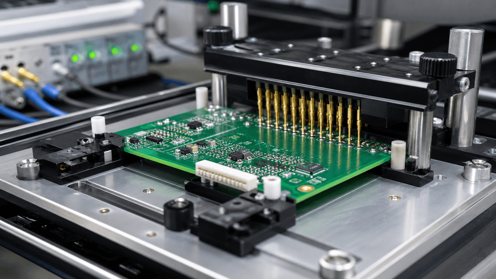
In-Circuit Test (ICT) / Bed-of-Nails Fixture
An in-circuit test fixture, often called a bed-of-nails jig, uses an array of spring-loaded pogo pins precisely aligned to the board’s test points. When the board is pressed into the fixture, every pin contacts its assigned node simultaneously. The ICT system then sweeps through resistance, capacitance, diode orientation and component value checks across hundreds or thousands of nodes in seconds, identifying shorts, opens, wrong values and missing components.
ICT fixtures are the preferred approach for high-volume production because test time per board is short – often under 30 seconds – and coverage can exceed 90% of populated nodes on a well-designed board. The trade-off is upfront fixture cost: a custom ICT fixture for a moderately complex board typically runs several thousand dollars, and the fixture needs to be updated whenever the PCB layout changes significantly. This makes ICT most economical at volumes where the per-unit savings in reduced rework justify the fixture investment.
Programming and Calibration Fixture
A programming fixture connects to the board’s debug or programming interface (JTAG, SWD, UART boot loader or production flash programming port) to load firmware and, where required, write calibration data to non-volatile memory. Programming fixtures are often built as standalone jigs used early in the production sequence, before functional or ICT testing. They are also the simplest and most cost-effective jig type to build.
Flying Probe Testing
A flying probe tester moves a small number of motorised probes – typically two to six – over the board surface, contacting test pads and component leads in sequence. Unlike a bed-of-nails fixture, a flying probe machine requires no custom fixture: test programs are generated from PCB design data, and setup time is measured in hours rather than weeks. The trade-off is speed: flying probe is significantly slower per board than ICT, making it practical for prototypes, NPI boards and low-volume production but uneconomical at scale. Flying probe is also well-suited to boards with high component density where pogo-pin access is constrained. For more detail on the flying probe versus bed-of-nails trade-off, see this comparison from AllPCB.
When to Invest in a Custom PCB Test Jig
The question most hardware product teams face is not whether to test, but at what volume a dedicated test fixture makes financial sense compared to manual testing or flying probe.
A rough framework for the decision:
- Under 50 units/month: Flying probe or manual bench testing is usually adequate. The cost of a custom jig will not be recovered across the production run.
- 50-200 units/month: A functional test jig becomes economical, particularly if the board has known failure modes or the product operates in an environment where field returns are costly (industrial, medical, mission-critical).
- 200+ units/month: ICT or a combined ICT-plus-FCT strategy pays back quickly. At this volume, even a modest first-pass yield improvement of two to three percentage points translates to meaningful savings in rework labour and component cost across a production run.
- Any volume – regulatory or quality system requirement: Products requiring IEC 60601, AS/NZS standards, CE/FCC certification or ISO 9001 production documentation often need a formalised test record per unit, which requires a structured jig regardless of volume.
Real-world production data supports the investment case. Published case studies from electronics contract manufacturers show first-pass yield improvements from 88% to over 94% after adding structured ICT and functional testing, saving over $100,000 AUD annually in rework and scrap at mid-volume production rates. Field failure rates on products with combined ICT and FCT coverage have been reported at 30-50% lower than products tested by visual inspection and manual checks alone.
The point at which a dedicated test fixture pays for itself can usually be calculated directly from your projected production volume, current rework rate and the cost of a warranty return in your specific market.
Design for Testability: Why It Must Come Early
The most common and most expensive mistake in PCB test jig development is treating testability as a concern to address after the board layout is finalised. By that point, the decisions that determine test coverage – test point placement, access clearance for pogo pins, circuit topology that allows individual components to be isolated for in-circuit measurement – have already been made.
Design for testability (DFT) is a set of PCB layout practices that make a board compatible with automated test fixtures. Key DFT principles include:
- Test point placement: Dedicated test pads on one side of the board, spaced to a defined grid (typically 2.54mm or 1.27mm pitch), accessible to the fixture’s pogo pins without mechanical interference from tall components or heatsinks.
- Net coverage: Every net that needs to be measured by ICT must have a reachable test point. Nets with no test point cannot be checked by any pogo-pin-based fixture.
- Power sequencing: Power rails should be accessible independently for ICT measurement. Boards where power rails cannot be isolated create false readings during in-circuit component testing.
- Programming access: A JTAG or SWD header, or clearly documented boot-loader pins, that can be reached by a programming fixture pogo pin without disturbing adjacent components.
- Connector location: Mating connectors used during functional test (for power input, signal injection or loopback) positioned on the board edge or in areas that do not conflict with the fixture’s mechanical clamp.
For product teams working with a design partner, the right time to discuss DFT requirements is during the PCB layout phase – not after the gerbers have been sent to the contract manufacturer. Zeus Design’s approach is to define the test strategy at the same time as the circuit design, so that DFT constraints are built into the PCB layout from the start rather than retrofitted at extra cost and delay.
Technical and Commercial Risks Without a Test Jig
Hardware teams that go to production without a structured PCB test jig face a predictable set of risks:
- Undetected assembly defects: Solder bridges, cold joints, wrong-value passives and reversed polarity components pass visual inspection but fail intermittently under temperature, vibration or electrical load. These are the defects most often found as DOA (dead on arrival) units or early field returns.
- Batch escapes: Without per-unit test records, a systematic assembly problem – a wrong tape-and-reel, a pick-and-place misalignment that affected an entire panel – can escape the entire production run before it is detected. The cost of a product recall or a large warranty return batch is typically far greater than the cost of the jig that would have caught it.
- No production data: Manual visual checks produce no structured data. A test jig produces per-unit pass/fail logs, failure type distributions and yield metrics. That data is essential for feeding back to the contract manufacturer, identifying component quality issues and demonstrating due diligence to customers or certification bodies.
- Scaling cost: Manual testing labour scales linearly with volume. A jig scales almost flat after the upfront development cost, so the per-unit test cost falls sharply as volume increases.
Zeus Design’s Approach to PCB Test Jig Development
Zeus Design develops custom PCB test jigs as part of its electronics design and production readiness service. The test fixture is developed alongside the PCB design and firmware – not as a separate project after the board is already in production – which means DFT requirements are built into the layout from the start.
The typical engagement covers:
- Test strategy definition: Working with the product team to define what the fixture must verify, what the pass/fail criteria are, and which fixture type (FCT, ICT, programming fixture or a combination) fits the production volume and budget.
- DFT review during PCB layout: Confirming that the board layout includes sufficient test point access, correct test pad dimensions and adequate clearance for the chosen fixture type before the design is finalised.
- Fixture design and build: Mechanical design of the housing, alignment tooling and clamping mechanism; custom interface PCB or harness connecting test points to the test controller; firmware or PC-side test software that sequences the stimulus, measures responses and logs results.
- Validation and commissioning: Running the completed fixture on known-good and known-bad boards to confirm it correctly classifies units, then handing over documentation and a calibration procedure to the production team.
This integrated approach avoids the common scenario where a test fixture is ordered as an afterthought, only to find that the PCB layout does not support the required test coverage – or that the firmware and hardware were developed by different parties and the test software cannot drive the board correctly.
Zeus Design also connects test jig work to the broader design for manufacture and rapid prototyping services, meaning the same team that designed the board is responsible for ensuring it can be tested efficiently at production volume. For Australian hardware teams moving from prototype to production, this reduces the number of handoffs and the risk of gaps between design, test and manufacturing readiness.
FAQs
What is a PCB test jig and what does it do?
A PCB test jig is a custom fixture that holds an assembled circuit board, makes precise electrical contact with its test points, and runs automated checks to verify the board meets its functional and electrical specification. It replaces manual bench testing with a repeatable, operator-independent process, producing a structured pass/fail result with traceability data for every unit tested.
How much does a PCB test jig cost to develop?
Development cost varies widely depending on fixture type and board complexity. A simple functional test jig or programming fixture for a low-complexity board may cost a few thousand dollars. A full in-circuit test fixture for a complex multilayer board with hundreds of test points can run to ten thousand dollars or more. The investment is typically recovered quickly through reduced rework and warranty return costs once production volume justifies it. See Zeus Design’s electronics design service for a project-specific estimate.
When in the product development process should a test jig be designed?
Test jig design should begin during the PCB layout phase, not after the board has been sent to manufacture. Design for testability (DFT) decisions – test point placement, net access, programming port location – must be made while the PCB layout can still be modified. Leaving jig design until after the first production run typically means retrofitting test points or accepting reduced coverage.
What is the difference between a functional test jig and an in-circuit test fixture?
A functional test jig powers the board and exercises it end-to-end, confirming it behaves correctly as a complete system. An in-circuit test (ICT) fixture, also called a bed-of-nails fixture, uses pogo pins to access individual nodes and checks component values, shorts and opens without fully powering the board. ICT is faster and suited to high-volume component-fault detection; FCT is the definitive check that the product works as intended.
What is a bed-of-nails PCB test fixture?
A bed-of-nails fixture is the most common type of in-circuit test jig. It contains an array of spring-loaded pogo pins, each aligned to a specific test point on the PCB. When the board is pressed into the fixture, all pins contact simultaneously, allowing the ICT system to measure every node in parallel in a matter of seconds. It is the preferred approach for high-volume production where short per-unit test time and broad coverage are both required. More detail on the technology is available from the in-circuit testing reference on Wikipedia.
Can a PCB test jig reduce warranty returns?
Yes – structured board-level testing catches assembly defects that would otherwise reach customers. Published production data shows that combining in-circuit and functional testing reduces field failure rates by 30-50% compared to visual inspection alone. The earlier a defect is caught in the production flow, the lower the cost to fix it, and the smaller the risk of batch escapes that trigger large-scale warranty claims.
Does Zeus Design develop test jigs for boards designed elsewhere?
Zeus Design’s preferred approach is to develop test jigs alongside the PCB design and firmware, which ensures DFT requirements are built into the layout from the start. For boards designed externally, Zeus Design can review the existing design for testability and develop a fixture for it, though coverage may be limited by the available test point access. Contact Zeus Design to discuss your specific situation.
Conclusion
A PCB test jig is not a nice-to-have for serious production runs – it is the mechanism by which defects are caught at the lowest possible cost, yield is tracked and improved, and the risk of a field failure or batch recall is contained. The decision about which fixture type to use and when to invest is directly tied to your volume, your product’s failure modes and the cost of a warranty return in your market.
The most important principle is timing: DFT decisions made during PCB layout determine what a jig can check. Teams that address testability late in the design process typically pay more for less coverage. Building test strategy into the design from the start – as part of a fully integrated electronics design engagement – is the most efficient path from prototype to reliable production.
If you are planning a production transition and need to define a test strategy, design a custom fixture or review an existing board for testability, Zeus Design’s test jig development service is part of the same electronics design and DFM engagement that takes your product from concept to production-ready hardware.


0 Comments