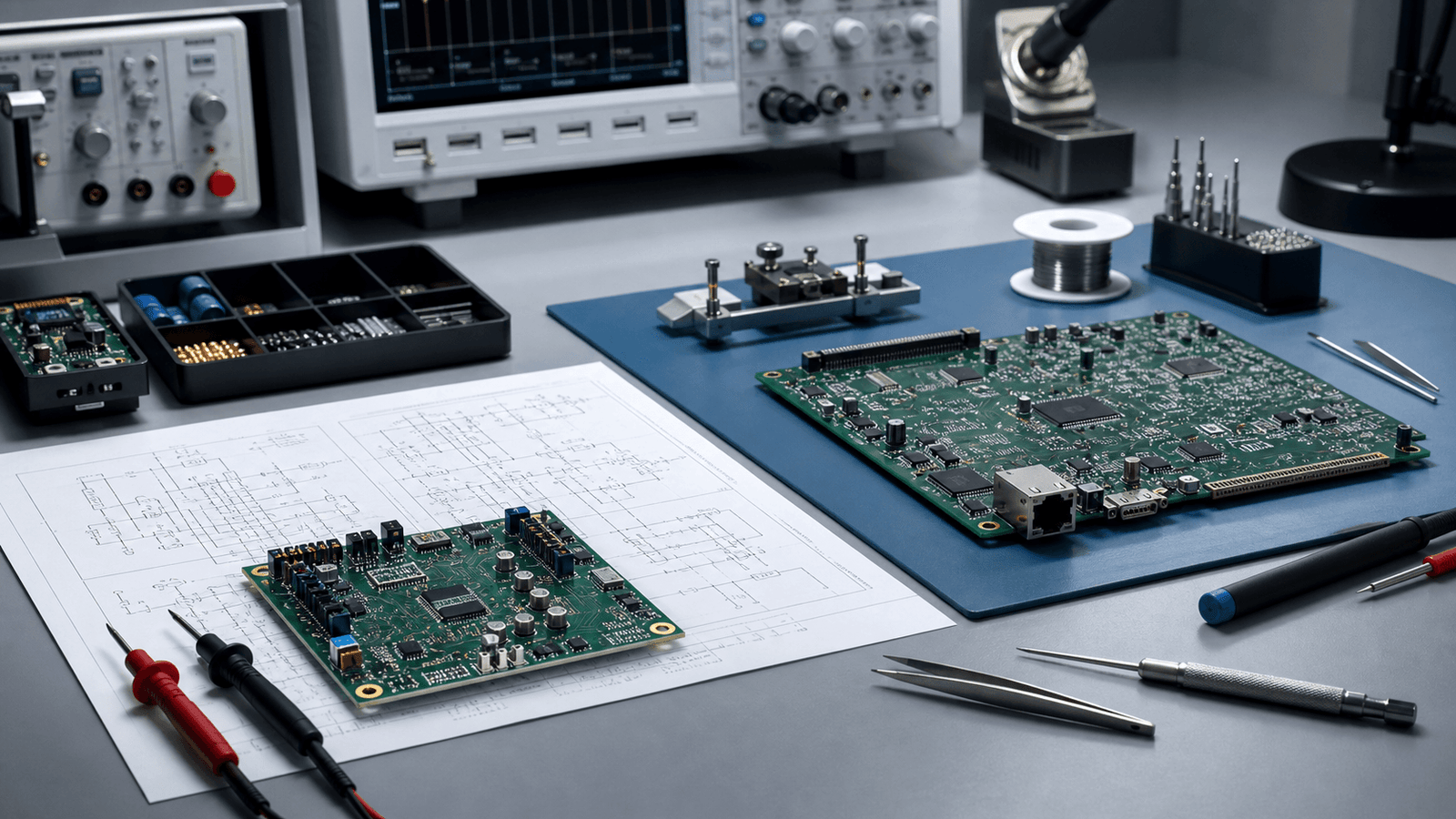
PCB solutions cover the full range of services a hardware team needs to turn a schematic into a manufacturable, tested circuit board – from initial layout and stack-up planning through prototyping, DFM review and production handover. This guide is written for startup founders, product managers and engineering leads who are evaluating what PCB services they actually need, what risks to plan for, and how to choose a design partner that can carry the work from concept through to volume. Zeus Design offers integrated circuit board design, rapid prototyping and DFM as a local Australian service, which removes the coordination overhead that comes with splitting design, fab and assembly across multiple vendors.
TL;DR
- PCB solutions span several distinct services: schematic capture, PCB layout, prototyping, DFM review, and production support – not all providers cover every step.
- Hardware startups typically need design-led PCB support rather than just fabrication; the design decisions made early drive production cost and yield later.
- Rapid prototyping validates electrical function and mechanical fit before committing to volume; skipping it is the most common source of expensive board respins.
- DFM (Design for Manufacture) review catches layout and component choices that would cause assembly failures or added cost at volume – it should happen before sending files to a fab, not after.
- An integrated design-and-prototyping partner reduces handoff risk; split models (design here, fab there) introduce version-control and specification gaps.
- Zeus Design handles circuit board design, PCB layout, rapid prototyping and DFM for Australian product teams, with embedded software and IoT connectivity available in the same engagement.
Why PCB Solutions Matter More Than PCB Fabrication
Most early-stage hardware teams search for “PCB solutions” when they realise their product needs more than a board house. Fabrication – having a factory produce your Gerbers – is only one part of the problem. Before files can go to a fab, someone needs to design the schematic, lay out the board, plan the layer stack-up, manage component selection, and verify that the design will assemble reliably at the quantities and costs the business model requires.
For startups and product companies, the gap is usually in the design layer, not the manufacturing layer. Offshore fabs are accessible and competitive on price. What is harder to find – especially in Australia – is a design partner who can take a product concept, produce a manufacturable PCB, prototype it quickly, and then hand over clean, production-ready files without requiring the client to manage multiple vendors across time zones.
This guide covers what each PCB service layer involves, which risks to manage at each stage, and what a complete set of PCB solutions looks like for a team building a hardware product in 2026.
What PCB Solutions Actually Include
The term covers a spectrum. Understanding which services you need – and which are already handled internally – helps avoid overpaying for things you do not need and, more importantly, avoids skipping things that protect production outcomes.
Schematic Design and Circuit Design
Before a PCB can be laid out, the circuit must be designed at the schematic level. This involves selecting and specifying components, defining the electrical topology, confirming power budgets, and creating a logical representation of the circuit that a PCB layout engineer can translate into a physical board.
For hardware startups without an in-house electronics engineer, schematic design is typically the first service required. Errors at this stage – wrong component ratings, inadequate power sequencing, missing protection circuits – cascade into every downstream stage and are expensive to correct after a prototype has been built.
Zeus Design’s electronics design service covers end-to-end circuit design from concept, including component selection, schematic capture and design review before layout begins.
PCB Layout
PCB layout translates the schematic into a physical board – placing components, routing traces, managing layer stack-ups, and ensuring the board meets both electrical performance requirements and the capabilities of the target fabrication process.
Layout quality has a direct effect on signal integrity, EMC performance, thermal behaviour and assembly yield. A board that is electrically correct at schematic level can still fail in the field if trace routing introduces noise on high-speed signals, power planes are poorly planned, or component placement makes rework difficult during prototyping.
Key decisions at layout stage include: number of layers, via strategy, copper pours, keepouts, impedance-controlled traces (critical for USB, Ethernet, RF and DDR interfaces), and component orientation for automated assembly. Cadence’s guidance on DFM analysis covers how layout decisions interact with fab capabilities in detail.
Zeus Design’s circuit board design and PCB layout service handles multilayer boards, signal integrity, EMC-aware design and full DFM preparation.
Rapid Prototyping
Rapid PCB prototyping produces small quantities of assembled boards – typically 1 to 10 units – to validate that the design works electrically and mechanically before ordering volume production. For startups, prototype boards are used to test core functionality, demonstrate to investors, run regulatory pre-compliance checks, and surface any design errors before they are locked into a production BOM.
Quick-turn prototype services can deliver assembled boards within one to two weeks for most designs. The cost per board at prototype quantities is significantly higher than volume, but the purpose is learning – finding and fixing issues while changes are still cheap.
Common reasons prototypes fail include incorrect footprints, component substitutions that change the BOM without updating the schematic, and layout errors that only show up under real operating conditions (heat, vibration, RF interference). A prototype stage that surfaces these issues early is not a failure – it is the expected and valuable outcome.
Zeus Design’s rapid electronics and PCB prototyping service covers proof-of-concept builds through to functional pre-production prototypes, with turnaround times suited to validation-paced development cycles.
Design for Manufacture (DFM) Review
DFM review is the process of checking a PCB design against the capabilities and constraints of the target assembly and fabrication process before files are sent for production. It catches issues that would cause assembly failures, added cost, or reduced yield at volume – not errors that affect electrical function, but errors that affect how reliably the board can be built.
Typical DFM findings include: component clearances that are too tight for pick-and-place, pad sizes that are out of spec for reflow soldering, via-in-pad designs that require tented vias, courtyard violations, insufficient test point access, and footprints that do not match the actual component body. Sierra Circuits’ DFM checklist gives a thorough overview of the categories of issues to check.
DFM review should happen before sending files to a fabricator, not after receiving boards back. A DFM issue caught in review costs hours; one caught at the assembly line costs a production run and the lead time to respun boards.
Bill of Materials (BOM) and Component Sourcing
A PCB design is only as manufacturable as its BOM. Component availability, lead times, lifecycle status and pricing all affect whether a board can actually be built when you need it and at the cost you planned. Designing around components that are end-of-life, single-sourced, or subject to long lead times introduces supply chain risk that surfaces at the worst possible time – during a production run.
BOM management as part of PCB solutions means checking component lifecycle status during design, identifying approved alternates, and ensuring the final BOM maps to components that are available in the quantities and timeframes required. This is a design-stage activity, not a procurement one.
Production Handover and Documentation
A complete set of PCB solutions ends with a clean handover package: fabrication files (Gerbers, drill files, IPC-2581 or ODB++ depending on the fab), assembly files (pick-and-place, assembly drawings, BOM with manufacturer part numbers), and any test documentation. This documentation package is what a contract manufacturer needs to build your board reliably, in volume, without constant clarification requests.
Gaps in the handover package – undocumented design intent, missing tolerances, incomplete BOM – create delays, cost overruns and quality issues at production that are avoidable with proper documentation practice during design.
When a Startup Needs Each Service
Not every engagement starts at the same point. Understanding where your project sits determines which PCB services you actually need right now versus which come later.
Concept to First Prototype
At this stage you have a product concept and possibly a rough block diagram or reference design, but no completed schematic. You need circuit design, PCB layout and a rapid prototype build. The goal is to prove the core electrical concept works on real hardware.
This stage should be treated as an exploration – expect iteration, plan for at least two prototype revisions, and avoid spending heavily on enclosures or packaging until the electronics are validated. Most schedules that slip at prototype stage do so because teams underestimate the number of revisions required or start too late.
Improving an Existing Design
Some teams come with a working design that needs refinement – cost reduction, improved EMC performance, a layout rework for a new form factor, or preparation for a higher-volume production run. Here the need is typically layout redesign and DFM review rather than circuit design from scratch.
DFM is especially valuable at this stage. A design that worked for 100 units at a local assembler may not work cost-effectively at 5,000 units through a contract manufacturer with different equipment and tolerances.
Scaling from Prototype to Production
Moving from a validated prototype to production-ready files involves DFM review, BOM rationalisation, production documentation and, often, layout revisions to support volume assembly processes. This is where the cost of early design decisions becomes visible – a board designed without assembly considerations typically needs significant rework before a CM can quote it reliably.
Zeus Design supports this transition through its electronics design and DFM service, which includes production handover documentation and review against target fabrication and assembly specifications.
Technical and Commercial Risks to Manage
PCB projects fail or run over budget for predictable reasons. Managing these risks early is more effective than recovering from them later.
Insufficient Prototyping Budget
Prototype builds are expensive per unit. Teams with tight budgets sometimes reduce prototype quantities to the point where there are not enough boards to find all the issues before committing to production. Building five boards and then discovering a systematic assembly issue on all five is a worse outcome than building ten and finding it while there is still time to reorder.
Component End-of-Life During Development
Long development cycles – common for complex hardware products – create risk that components specified at design start will be discontinued or become unavailable by production. Checking lifecycle status at the start of design and identifying alternates is a standard practice that is frequently skipped under schedule pressure.
Splitting Design and Prototyping Across Vendors
Using one firm for PCB design and another for prototyping introduces handoff risk. File format incompatibilities, unclear design intent, and version control issues between vendors are common sources of errors that would not exist if the same team produced the design and built the prototype. For early-stage products especially, the efficiency of a single integrated team outweighs any price advantage from splitting the work.
Skipping Pre-Compliance EMC Review
EMC compliance (required for most electronic products sold in Australia) is heavily influenced by PCB layout – ground plane integrity, filtering, trace routing near switching circuits, and connector placement all affect radiated and conducted emissions. A layout that is not EMC-aware typically requires expensive board respins after pre-compliance testing identifies failures. Australia’s electrical equipment regulatory requirements apply to most electronics products sold in the domestic market.
Underspecifying the Stack-Up
Layer count and stack-up decisions affect signal integrity, impedance control, EMC performance and fabrication cost. A two-layer board is cheaper but limits routing options and makes power delivery and EMC harder to manage on complex designs. Going straight to a six-layer board for a design that could work on four adds cost. Stack-up decisions made without analysis of the actual design requirements cause avoidable cost or performance issues.
Zeus Design: Integrated PCB Solutions for Australian Product Teams
Zeus Design provides circuit board design, PCB layout, rapid prototyping and DFM as an integrated service for Australian startups and product companies. The integration matters because the design, prototype and DFM stages are not cleanly separable – decisions made at layout directly affect prototyping outcomes, and DFM findings often require layout revisions before a board is ready for production.
Working with a single team across these stages avoids the version control and specification gaps that arise when design and prototyping are handled by separate vendors. It also means that engineering knowledge built up during circuit design – the rationale for specific component choices, the signal integrity constraints on certain traces, the thermal management approach – stays with the team reviewing DFM findings and building prototypes rather than being lost in handoffs.
For teams that need embedded software alongside the hardware, Zeus Design’s embedded software development service covers firmware and microcontroller software developed in parallel with the hardware, which removes the integration delays that occur when firmware development starts only after hardware is available.
For IoT products that require wireless connectivity and cloud integration, Zeus Design handles the full hardware-to-cloud stack – PCB design, firmware, connectivity and cloud backend – as a single engagement.
Zeus Design operates from Australia, which means project communication happens in Australian business hours, contracts are governed by Australian law, and there is no language or time-zone overhead. For teams building products for the Australian market or working under Australian regulatory frameworks, a local partner who understands ACMA and RCM requirements is a practical advantage.
How PCB Solutions Connect to Related Services
PCB design and prototyping rarely exist in isolation in a hardware product project. The most common adjacent services are:
- Embedded software / firmware – The PCB provides the hardware platform; firmware must be developed to run on it. Co-developing hardware and firmware avoids the common problem of hardware being delivered to a firmware team that then discovers peripheral configurations, timing requirements, or pin assignments that need board-level changes.
- IoT connectivity – Products with wireless communication (Wi-Fi, Bluetooth, cellular, LPWAN) require antenna design, RF layout, and connectivity stack decisions to be made at PCB design stage. Adding connectivity as an afterthought typically requires a board respin.
- Test jig development – Production testing requires fixtures that make electrical contact with the assembled board. Test jigs should be designed alongside the PCB, with test point placement agreed before layout is finalised. Retrofitting test access to an existing design is always more expensive.
- Mobile app or cloud backend – Connected products need software on both ends of the connection. Planning the cloud architecture and API while the hardware is being designed prevents integration surprises later in the project.
FAQs
What are PCB solutions and what do they include?
PCB solutions refer to the range of services covering the design, prototyping, review and production preparation of printed circuit boards. At minimum this includes PCB layout (translating a schematic into a physical board), but complete PCB solutions also cover schematic and circuit design, DFM review, BOM management, rapid prototyping and production documentation. The scope you need depends on how far along your design is and what internal engineering capability your team has.
Do I need a PCB design service or just a PCB fabrication service?
If you already have completed, DFM-reviewed Gerber files, you need fabrication. If you have a schematic or concept but no layout, or if you have a layout that has not been reviewed for manufacturability, you need a design service first. Most hardware startups need design and prototyping rather than fabrication alone – the fabrication step is typically handled by the design partner or a contract manufacturer downstream.
How many prototype iterations should I budget for?
Most hardware products require two to three prototype iterations before a design is production-ready. The first prototype validates core electrical function. The second typically addresses layout issues, component substitutions and any firmware integration problems identified during testing. A third revision is common on more complex designs or where regulatory pre-compliance testing surfaces EMC issues. Planning for two revisions as a minimum avoids the schedule pressure that comes from assuming the first prototype will be the last.
When should DFM review happen in the project timeline?
DFM review should happen after layout is complete and before files are sent to a fabricator – ideally before the final prototype is built, so DFM findings can be incorporated rather than deferred to a separate production-prep revision. Running DFM review after a prototype is already in production risks discovering assembly issues that require a board respin to fix. See Zeus Design’s electronics design and DFM service for how DFM fits into an integrated PCB project.
What is the difference between PCB layout and circuit board design?
Circuit board design is the broader term covering both schematic capture (defining the circuit) and PCB layout (physically placing and routing that circuit on a board). PCB layout is the specific task of translating a completed schematic into a physical board file. Some engineers and firms handle both; others specialise in layout only. For hardware startups, working with a partner who handles the full scope – from schematic through to layout and DFM – reduces the coordination overhead of managing separate specialists.
Can Zeus Design handle PCB design and firmware in the same project?
Yes. Zeus Design develops embedded software and firmware alongside hardware, which means the firmware team is involved during PCB design rather than receiving a finished board and starting from scratch. Co-development avoids the integration delays and hardware revision requests that arise when firmware development begins only after hardware is delivered. See the embedded software development service for details.
What should I look for when choosing a PCB solutions provider in Australia?
Look for a provider who covers design, prototyping and DFM as integrated services rather than just one piece of the stack. Check that they have experience with the type of product you are building – consumer IoT, industrial electronics, medical devices, and power electronics each have different design requirements. Confirm they understand Australian regulatory requirements (RCM, ACMA) and can support pre-compliance planning. An Australian-based provider offers the practical advantages of aligned business hours, local contracts and accountability under Australian law.
Conclusion
PCB solutions for hardware startups and product companies span more than fabrication. The design, layout, DFM and prototyping stages are where the decisions that determine cost, quality and schedule outcomes are made – and where the most value is added by an experienced engineering partner.
For Australian product teams, working with a local provider who handles the full stack – from circuit design through prototyping, DFM and production handover – removes the coordination overhead and handoff risk of splitting the work across multiple vendors. Zeus Design provides these services as an integrated offering, with embedded software, IoT connectivity and cloud development available in the same engagement for teams building connected products.
If you are at concept stage, mid-prototype or preparing for production scale-up, the circuit board design and rapid prototyping services are the right starting points. For questions about scope, timeline and fit, contact Zeus Design directly.




0 Comments